CC1101
SWRS061H Page 21 of 98
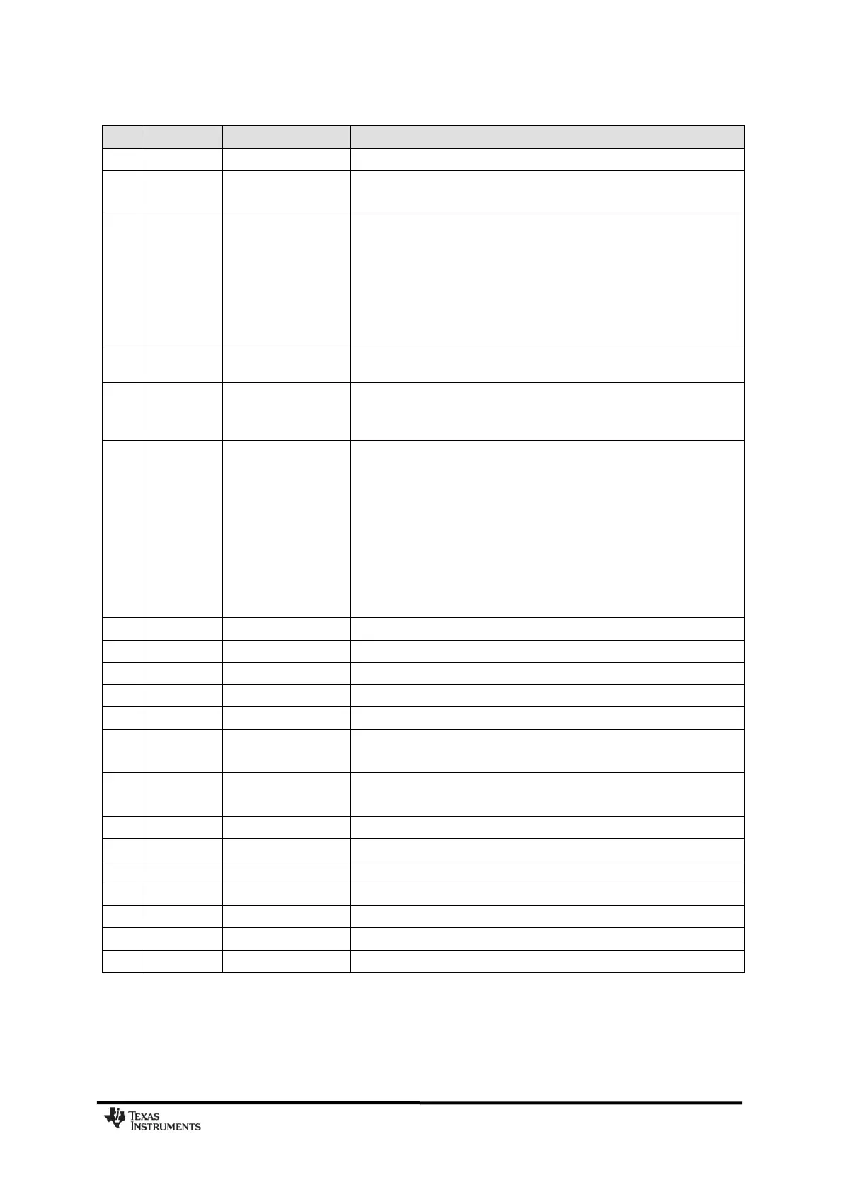
Serial configuration interface, clock input
Serial configuration interface, data output
Optional general output pin when CSn is high
Digital output pin for general use:
Test signals
FIFO status signals
Clear channel indicator
Clock output, down-divided from XOSC
Serial output RX data
1.8 - 3.6 V digital power supply for digital I/O‟s and for the digital core
voltage regulator
1.6 - 2.0 V digital power supply output for decoupling
NOTE: This pin is intended for use with the
CC1101
only. It can not be used
to provide supply voltage to other devices
Digital output pin for general use:
Test signals
FIFO status signals
Clear channel indicator
Clock output, down-divided from XOSC
Serial output RX data
Serial input TX data
Also used as analog test I/O for prototype/production testing
Serial configuration interface, chip select
Crystal oscillator pin 1, or external clock input
1.8 - 3.6 V analog power supply connection
1.8 - 3.6 V analog power supply connection
Positive RF input signal to LNA in receive mode
Positive RF output signal from PA in transmit mode
Negative RF input signal to LNA in receive mode
Negative RF output signal from PA in transmit mode
1.8 - 3.6 V analog power supply connection
1.8 - 3.6 V analog power supply connection
External bias resistor for reference current
Power supply connection for digital noise isolation
Ground connection for digital noise isolation
Serial configuration interface, data input
Table 19: Pinout Overview