CC1101
SWRS061H Page 27 of 98
reflow process, which may cause defects
(splattering, solder balling). Using “tented” vias
reduces the solder paste coverage below
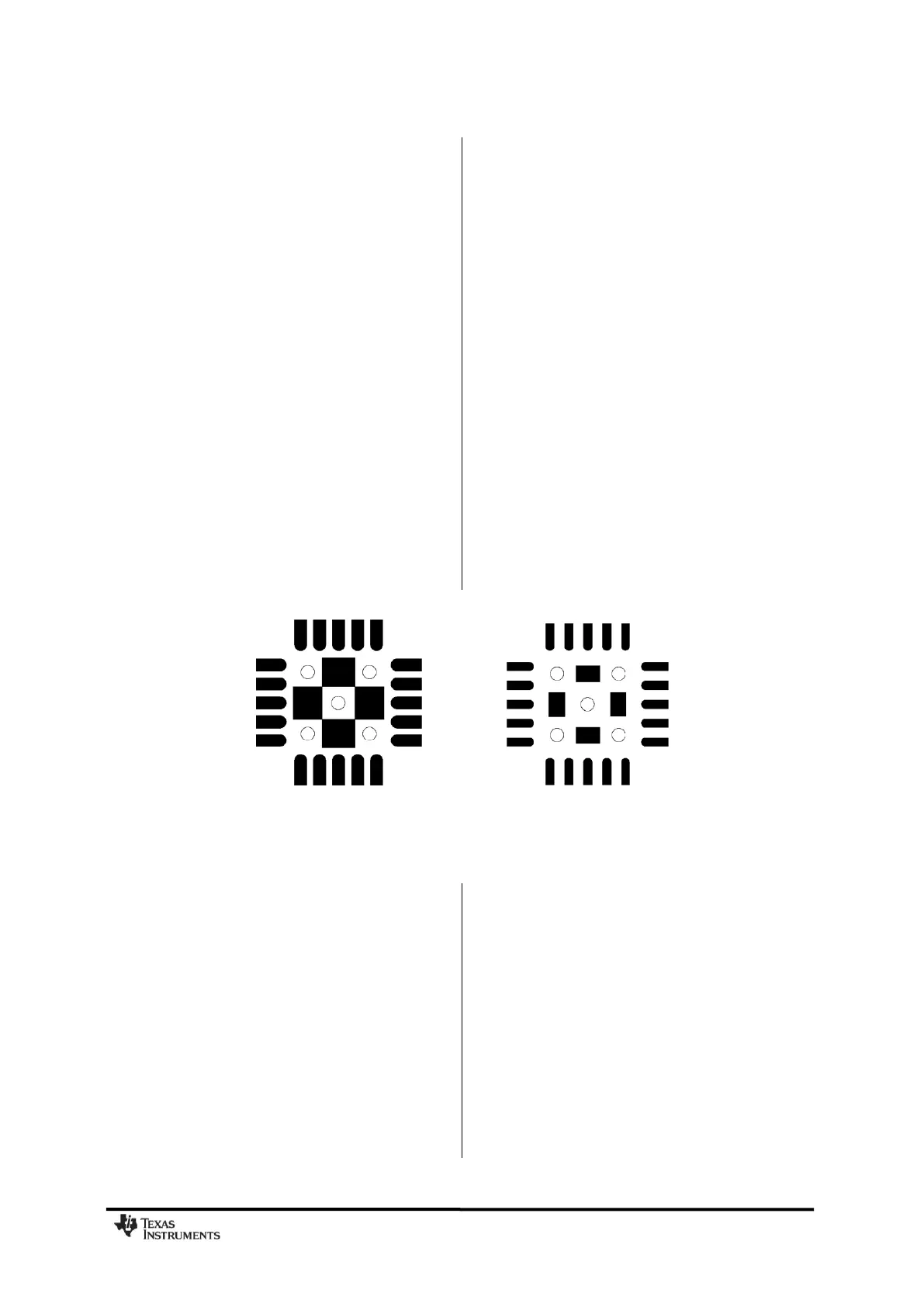
100%. See Figure 12 for top solder resist and
top paste masks.
Each decoupling capacitor should be placed
as close as possible to the supply pin it is
supposed to decouple. Each decoupling
capacitor should be connected to the power
line (or power plane) by separate vias. The
best routing is from the power line (or power
plane) to the decoupling capacitor and then to
the
CC1101
supply pin. Supply power filtering is
very important.
Each decoupling capacitor ground pad should
be connected to the ground plane by separate
vias. Direct connections between neighboring
power pins will increase noise coupling and
should be avoided unless absolutely
necessary. Routing in the ground plane
underneath the chip or the balun/RF matching
circuit, or between the chip‟s ground vias and
the decoupling capacitor‟s ground vias should
be avoided. This improves the grounding and
ensures the shortest possible current return
path.
Avoid routing digital signals with sharp edges
close to XOSC_Q1 PCB track or underneath
the crystal Q1 pad as this may shift the crystal
dc operating point and result in duty cycle
variation.
The external components should ideally be as
small as possible (0402 is recommended) and
surface mount devices are highly
recommended. Please note that components
with different sizes than those specified may
have differing characteristics.
Precaution should be used when placing the
microcontroller in order to avoid noise
interfering with the RF circuitry.
A CC1101DK Development Kit with a fully
assembled CC1101EM Evaluation Module is
available. It is strongly advised that this
reference layout is followed very closely in
order to get the best performance. The
schematic, BOM and layout Gerber files are all
available from the TI website ([1] and [2]).
Figure 12: Left: Top Solder Resist Mask (Negative). Right: Top Paste Mask. Circles are Vias
8 Configuration Overview
CC1101
can be configured to achieve optimum
performance for many different applications.
Configuration is done using the SPI interface.
See Section 10 below for more description of
the SPI interface. The following key
parameters can be programmed:
Power-down / power up mode
Crystal oscillator power-up / power-down
Receive / transmit mode
RF channel selection
Data rate
Modulation format
RX channel filter bandwidth
RF output power
Data buffering with separate 64-byte
receive and transmit FIFOs
Packet radio hardware support
Forward Error Correction (FEC) with
interleaving
Data whitening
Wake-On-Radio (WOR)
Details of each configuration register can be
found in Section 29, starting on page 66.
Figure 13 shows a simplified state diagram
that explains the main
CC1101
states together
with typical usage and current consumption.
For detailed information on controlling the