CC1101
SWRS061H Page 22 of 98
6 Circuit Description
BIAS
PA
RBIAS XOSC_Q1 XOSC_Q2
CSn
SI
SO (GDO1)
XOSC
SCLK
LNA
0
90
FREQ
SYNTH
ADC
ADC
DEMODULATOR
FEC / INTERLEAVER
PACKET HANDLER
RXFIFO
MODULATOR
TXFIFO
DIGITAL INTERFACE TO MCU
RADIO CONTROL
RF_P
RF_N
GDO2
GDO0 (ATEST)
RC OSC
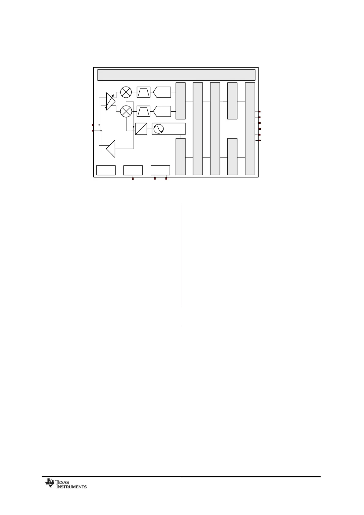
Figure 9:
CC1101
Simplified Block Diagram
A simplified block diagram of
CC1101
is shown
in Figure 9.
CC1101
features a low-IF receiver. The received
RF signal is amplified by the low-noise
amplifier (LNA) and down-converted in
quadrature (I and Q) to the intermediate
frequency (IF). At IF, the I/Q signals are
digitised by the ADCs. Automatic gain control
(AGC), fine channel filtering, demodulation,
and bit/packet synchronization are performed
digitally.
The transmitter part of
CC1101
is based on
direct synthesis of the RF frequency. The
frequency synthesizer includes a completely
on-chip LC VCO and a 90 degree phase
shifter for generating the I and Q LO signals to
the down-conversion mixers in receive mode.
A crystal is to be connected to XOSC_Q1 and
XOSC_Q2. The crystal oscillator generates the
reference frequency for the synthesizer, as
well as clocks for the ADC and the digital part.
A 4-wire SPI serial interface is used for
configuration and data buffer access.
The digital baseband includes support for
channel configuration, packet handling, and
data buffering.
7 Application Circuit
Only a few external components are required
for using the
CC1101
. The recommended
application circuits for
CC1101
are shown in
Figure 10 and
Figure 11. The external components are
described in Table 20, and typical values are
given in Table 21.
The 315 MHz and 433 MHz CC1101EM
reference design [1] use inexpensive multi-
layer inductors. The 868 MHz and 915 MHz
CC1101EM reference design [2] use wire-
wound inductors as this give better output
power, sensitivity, and attenuation of
harmonics compared to using multi-layer
inductors. Refer to design note DN032 [24] for
information about performance when using
wire-wound inductors from different vendors.
See also Design Note DN013 [15], which gives
the output power and harmonics when using
multi-layer inductors. The output power is then
typically +10 dBm when operating at 868/915
MHz.
7.1 Bias Resistor
The bias resistor R171 is used to set an accurate bias current.