EasyManuals Logo

Texas Instruments CC1101 User Manual

Texas Instruments CC1101
106 pages
To Next Page IconTo Next Page
To Previous Page IconTo Previous Page
Page #71 background imageLoading...
Page #71 background image
CC1101
SWRS061H Page 71 of 98
29.1 Configuration Register Details Registers with preserved values in SLEEP state
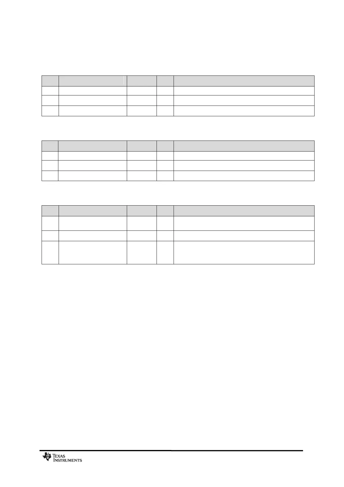
0x00: IOCFG2 GDO2 Output Pin Configuration
Bit
Field Name
Reset
R/W
Description
7
R0
Not used
6
GDO2_INV
0
R/W
Invert output, i.e. select active low (1) / high (0)
5:0
GDO2_CFG[5:0]
41 (0x29)
R/W
Default is CHP_RDYn (See Table 41 on page 62).
0x01: IOCFG1 GDO1 Output Pin Configuration
Bit
Field Name
Reset
R/W
Description
7
GDO_DS
0
R/W
Set high (1) or low (0) output drive strength on the GDO pins.
6
GDO1_INV
0
R/W
Invert output, i.e. select active low (1) / high (0)
5:0
GDO1_CFG[5:0]
46 (0x2E)
R/W
Default is 3-state (See Table 41 on page 62).
0x02: IOCFG0 GDO0 Output Pin Configuration
Bit
Field Name
Reset
R/W
Description
7
TEMP_SENSOR_ENABLE
0
R/W
Enable analog temperature sensor. Write 0 in all other register
bits when using temperature sensor.
6
GDO0_INV
0
R/W
Invert output, i.e. select active low (1) / high (0)
5:0
GDO0_CFG[5:0]
63 (0x3F)
R/W
Default is CLK_XOSC/192 (See Table 41 on page 62).
It is recommended to disable the clock output in initialization, in
order to optimize RF performance.

Table of Contents

Other manuals for Texas Instruments CC1101

Questions and Answers:

Question and Answer IconNeed help?

Do you have a question about the Texas Instruments CC1101 and is the answer not in the manual?

Texas Instruments CC1101 Specifications

General IconGeneral
BrandTexas Instruments
ModelCC1101
CategoryTransceiver
LanguageEnglish

Related product manuals