CC1101
SWRS061H Page 29 of 98
9 Configuration Software
CC1101
can be configured using the SmartRF
TM
Studio software [5]. The SmartRF Studio
software is highly recommended for obtaining
optimum register settings, and for evaluating
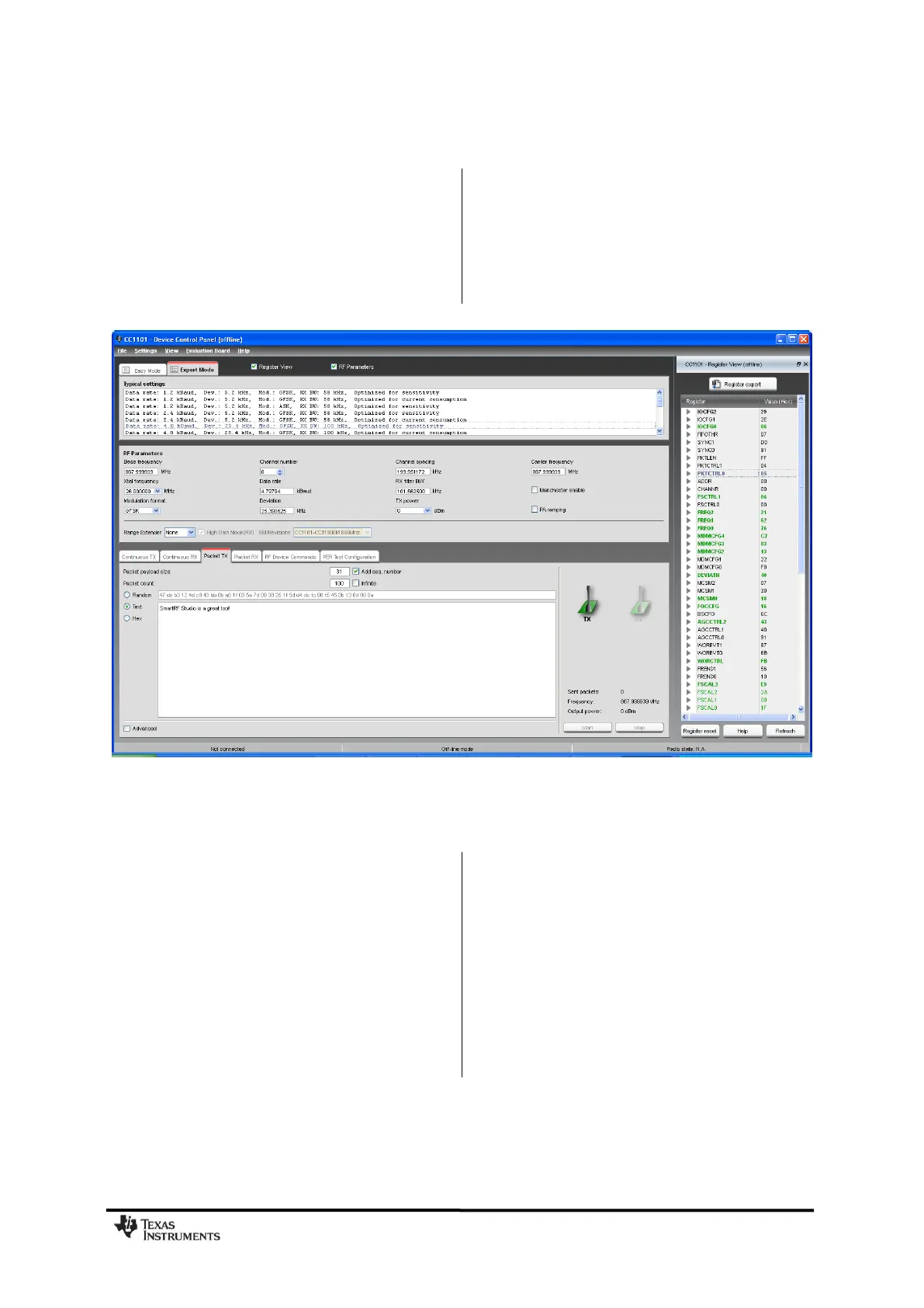
performance and functionality. A screenshot of
the SmartRF Studio user interface for
CC1101
is
shown in Figure 14.
After chip reset, all the registers have default
values as shown in the tables in Section 29.
The optimum register setting might differ from
the default value. After a reset all registers that
shall be different from the default value
therefore needs to be programmed through
the SPI interface.
Figure 14: SmartRF
TM
Studio [5] User Interface
10 4-wire Serial Configuration and Data Interface
CC1101
is configured via a simple 4-wire SPI-
compatible interface (SI, SO, SCLK and CSn)
where
CC1101
is the slave. This interface is
also used to read and write buffered data. All
transfers on the SPI interface are done most
significant bit first.
All transactions on the SPI interface start with
a header byte containing a R/W¯ bit, a burst
access bit (B), and a 6-bit address (A
5
– A
0
).
The CSn pin must be kept low during transfers
on the SPI bus. If CSn goes high during the
transfer of a header byte or during read/write
from/to a register, the transfer will be
cancelled. The timing for the address and data
transfer on the SPI interface is shown in Figure
15 with reference to Table 22.
When CSn is pulled low, the MCU must wait
until
CC1101
SO pin goes low before starting to
transfer the header byte. This indicates that
the crystal is running. Unless the chip was in
the SLEEP or XOFF states, the SO pin will
always go low immediately after taking CSn
low.