CC1101
SWRS061H Page 34 of 98
11 Microcontroller Interface and Pin Configuration
In a typical system,
CC1101
will interface to a
microcontroller. This microcontroller must be
able to:
Program
CC1101
into different modes
Read and write buffered data
Read back status information via the 4-wire
SPI-bus configuration interface (SI, SO,
SCLK and CSn)
11.1 Configuration Interface
The microcontroller uses four I/O pins for the
SPI configuration interface (SI, SO, SCLK and
CSn). The SPI is described in Section 10 on
page 29.
11.2 General Control and Status Pins
The
CC1101
has two dedicated configurable
pins (GDO0 and GDO2) and one shared pin
(GDO1) that can output internal status
information useful for control software. These
pins can be used to generate interrupts on the
MCU. See Section 26 on page 61 for more
details on the signals that can be
programmed.
GDO1 is shared with the SO pin in the SPI
interface. The default setting for GDO1/SO is
3-state output. By selecting any other of the
programming options, the GDO1/SO pin will
become a generic pin. When CSn is low, the
pin will always function as a normal SO pin.
In the synchronous and asynchronous serial
modes, the GDO0 pin is used as a serial TX
data input pin while in transmit mode.
The GDO0 pin can also be used for an on-chip
analog temperature sensor. By measuring the
voltage on the GDO0 pin with an external
ADC, the temperature can be calculated.
Specifications for the temperature sensor are
found in Section 4.7. With default PTEST
register setting (0x7F), the temperature sensor
output is only available if the frequency
synthesizer is enabled (e.g. the MANCAL,
FSTXON, RX, and TX states). It is necessary
to write 0xBF to the PTEST register to use the
analog temperature sensor in the IDLE state.
Before leaving the IDLE state, the PTEST
register should be restored to its default value
(0x7F).
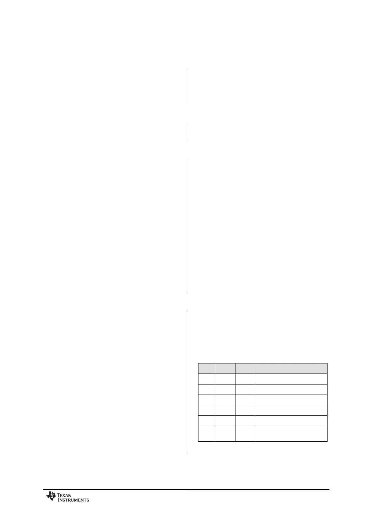
11.3 Optional Radio Control Feature
The
CC1101
has an optional way of controlling
the radio by reusing SI, SCLK, and CSn from
the SPI interface. This feature allows for a
simple three-pin control of the major states of
the radio: SLEEP, IDLE, RX, and TX. This
optional functionality is enabled with the
MCSM0.PIN_CTRL_EN configuration bit.
State changes are commanded as follows:
If CSn is high, the SI and SCLK are set to
the desired state according to Table 24.
If CSn goes low, the state of SI and SCLK
is latched and a command strobe is
generated internally according to the pin
configuration.
It is only possible to change state with the
latter functionality. That means that for
instance RX will not be restarted if SI and
SCLK are set to RX and CSn toggles. When
CSn is low the SI and SCLK has normal SPI
functionality.
All pin control command strobes are executed
immediately except the SPWD strobe. The
SPWD strobe is delayed until CSn goes high.
Chip unaffected by SCLK/SI
SPI mode (wakes up into
IDLE if in SLEEP/XOFF)
Table 24: Optional Pin Control Coding