CC1101
SWRS061H Page 20 of 98
4.8 DC Characteristics
T
A
= 25C if nothing else stated.
Table 17: DC Characteristics
4.9 Power-On Reset
For proper Power-On-Reset functionality the power supply should comply with the requirements in
Table 18 below. Otherwise, the chip should be assumed to have unknown state until transmitting an
SRES strobe over the SPI interface. See Section 19.1 on page 50 for further details.
Table 18: Power-On Reset Requirements
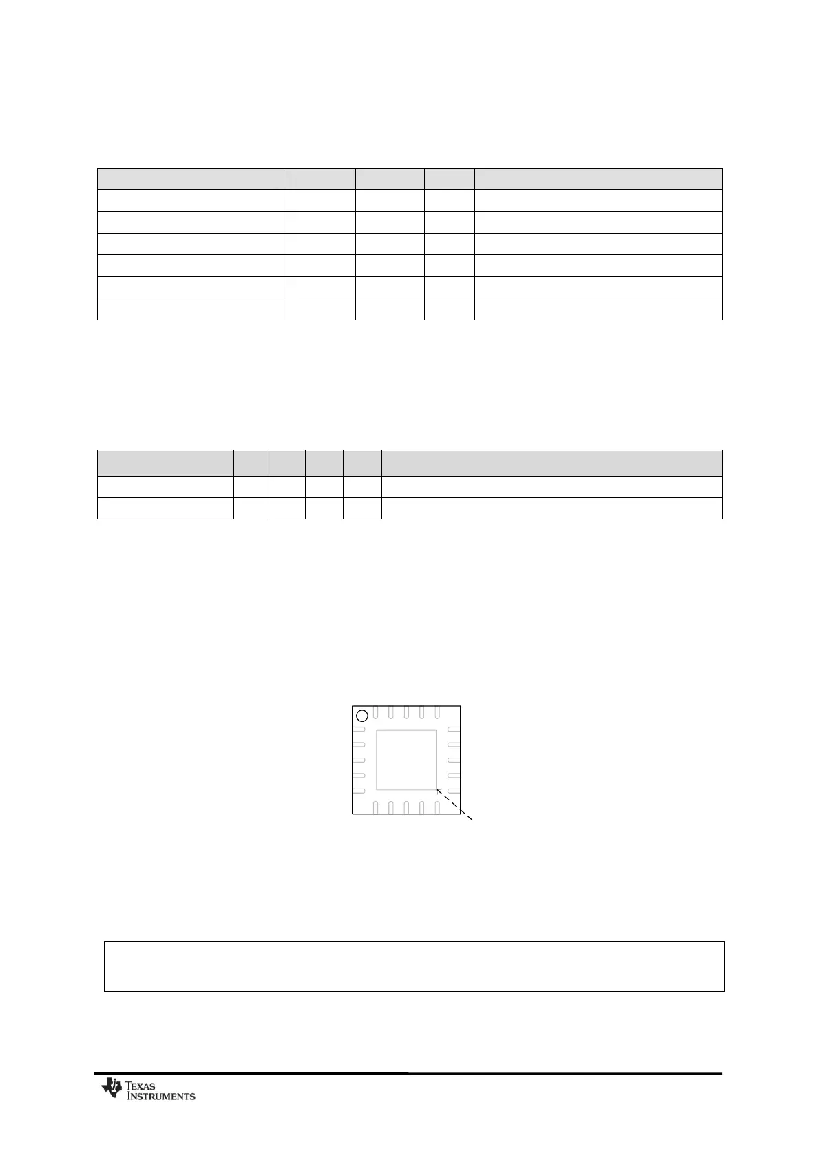
5 Pin Configuration
The
CC1101
pin-out is shown in Figure 8 and Table 19. See Section 26 for details on the I/O
configuration.
1
20 19 18 17 16
15
14
13
12
11
109876
5
4
3
2
GND
Exposed die
attach pad
SCLK
SO (GDO1)
GDO2
DVDD
DCOUPL
GDO0 (ATEST)
XOSC_Q1
AVDD
XOSC_Q2
AVDD
RF_P
RF_N
GND
AVDD
RBIAS
DGUARD
GND
SI
CSn
AVDD
Figure 8: Pinout Top View
.
For up to 4 mA output current
For up to 4 mA output current
From 0V until reaching 1.8V
Minimum time between power-on and power-off
Note: The exposed die attach pad must be connected to a solid ground plane as this is the main
ground connection for the chip