CC1101
SWRS061H Page 61 of 98
e.g 6
PA_POWER[2:0]
in FREND0 register
PATABLE(0)[7:0]
PATABLE(1)[7:0]
PATABLE(2)[7:0]
PATABLE(3)[7:0]
PATABLE(4)[7:0]
PATABLE(5)[7:0]
PATABLE(6)[7:0]
PATABLE(7)[7:0]
Index into PATABLE(7:0)
The PA uses this
setting.
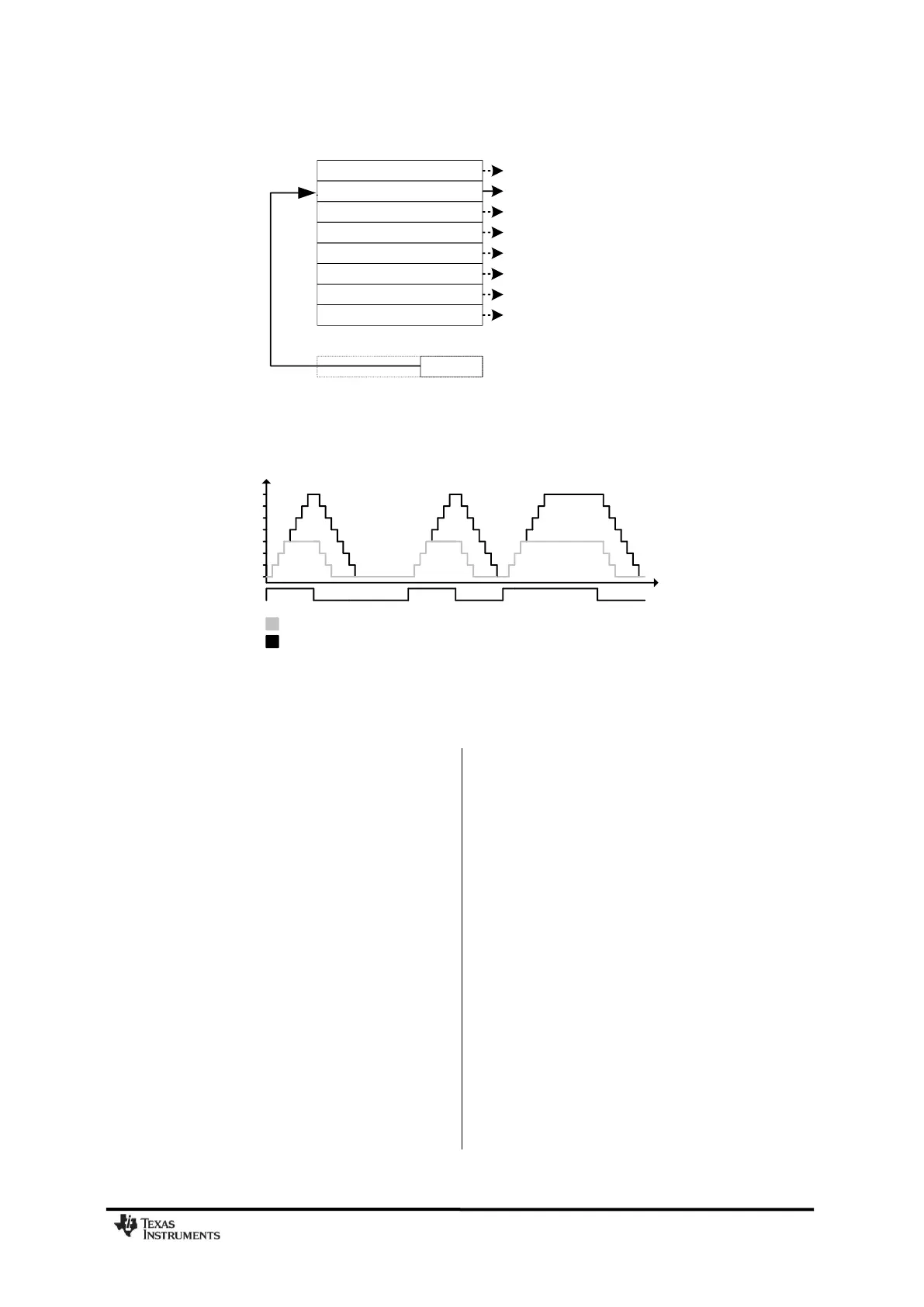
Settings 0 to PA_POWER are
used during ramp-up at start of
transmission and ramp-down at
end of transmission, and for
ASK/OOK modulation.
The SmartRF® Studio software
should be used to obtain optimum
PATABLE settings for various
output powers.
Figure 31: PA_POWER and PATABLE
11 0 0 0 1 0
Bit Sequence
1
FREND0.PA_POWER = 3
FREND0.PA_POWER = 7
Time
PATABLE[0]
PATABLE[1]
PATABLE[2]
PATABLE[3]
PATABLE[4]
PATABLE[5]
PATABLE[6]
PATABLE[7]
Output Power
Figure 32: Shaping of ASK Signal
26 General Purpose / Test Output Control Pins
The three digital output pins GDO0, GDO1,
and GDO2 are general control pins configured
with IOCFG0.GDO0_CFG,
IOCFG1.GDO1_CFG, and IOCFG2.GDO2_CFG
respectively. Table 41 shows the different
signals that can be monitored on the GDO
pins. These signals can be used as inputs to
the MCU.
GDO1 is the same pin as the SO pin on the
SPI interface, thus the output programmed on
this pin will only be valid when CSn is high.
The default value for GDO1 is 3-stated which
is useful when the SPI interface is shared with
other devices.
The default value for GDO0 is a 135-141 kHz
clock output (XOSC frequency divided by
192). Since the XOSC is turned on at power-
on-reset, this can be used to clock the MCU in
systems with only one crystal. When the MCU
is up and running, it can change the clock
frequency by writing to IOCFG0.GDO0_CFG.
An on-chip analog temperature sensor is
enabled by writing the value 128 (0x80) to the
IOCFG0 register. The voltage on the GDO0
pin is then proportional to temperature. See
Section 4.7 for temperature sensor
specifications.
If the IOCFGx.GDOx_CFG setting is less than
0x20 and IOCFGx_GDOx_INV is 0 (1), the
GDO0 and GDO2 pins will be hardwired to 0
(1), and the GDO1 pin will be hardwired to 1
(0) in the SLEEP state. These signals will be
hardwired until the CHIP_RDYn signal goes
low.
If the IOCFGx.GDOx_CFG setting is 0x20 or
higher, the GDO pins will work as programmed
also in SLEEP state. As an example, GDO1 is
high impedance in all states if
IOCFG1.GDO1_CFG=0x2E.