CC1101
SWRS061H Page 30 of 98
0
A5
A4
A3
A2
A0
A1
D
W
7
1
Read from register:
Write to register:
Hi-Z
X
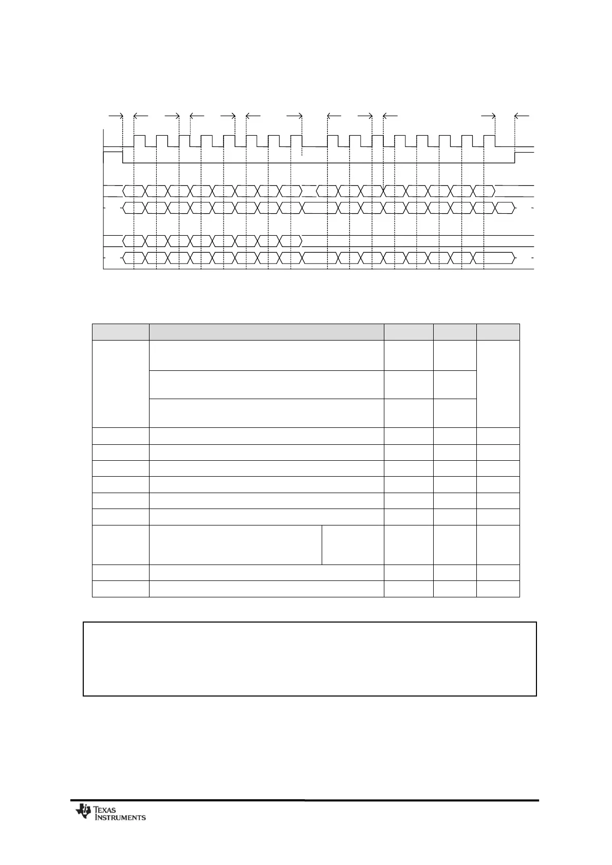
SCLK:
CSn:
SI
SO
SI
SO
Hi-Z
t
sp
t
ch
t
cl
t
sd
t
hd
t
ns
X
X
Hi-Z
X
Hi-Z
S7
X
D
W
6 D
W
5 D
W
4 D
W
3 D
W
2 D
W
1 D
W
0
B
S5
S4
S3 S2 S1 S0
S7
S6
S5 S4 S3
S2
S1 S0
B
B
A5 A4 A3 A2 A1 A0
S7
B S5 S4 S3 S2 S1 S0
D
R
7 D
R
6 D
R
5 D
R
4 D
R
3 D
R
2 D
R
1 D
R
0
Figure 15: Configuration Registers Write and Read Operations
SCLK frequency
100 ns delay inserted between address byte and data byte (single access), or
between address and data, and between each data byte (burst access).
SCLK frequency, single access
No delay between address and data byte
SCLK frequency, burst access
No delay between address and data byte, or between data bytes
CSn low to positive edge on SCLK, in power-down mode
CSn low to positive edge on SCLK, in active mode
Setup data (negative SCLK edge) to
positive edge on SCLK
(t
sd
applies between address and data bytes, and between
data bytes)
Single access
Burst access
Hold data after positive edge on SCLK
Negative edge on SCLK to CSn high.
Table 22: SPI Interface Timing Requirements
Note: The minimum t
sp,pd
figure in Table 22 can be used in cases where the user does not read
the CHIP_RDYn signal. CSn low to positive edge on SCLK when the chip is woken from power-
down depends on the start-up time of the crystal being used. The 150 μs in Table 22 is the
crystal oscillator start-up time measured on CC1101EM reference designs ([1] and [2]) using
crystal AT-41CD2 from NDK.