www.ti.com
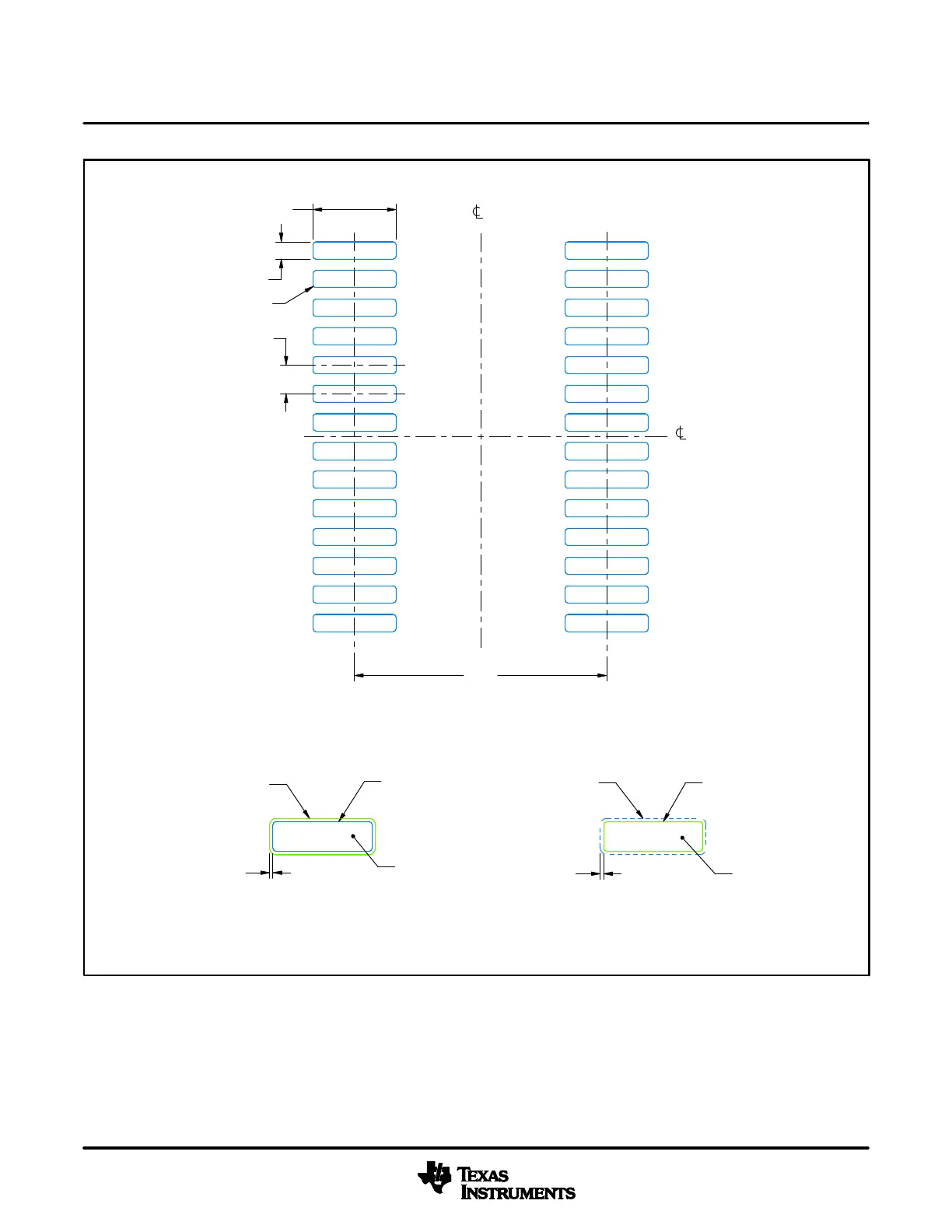
EXAMPLE BOARD LAYOUT
0.05 MAX
ALL AROUND
0.05 MIN
ALL AROUND
28X (1.45)
28X (0.3)
26X (0.5)
(4.4)
(R0.05) TYP
VSSOP - 1.1 mm max height
DGS0028A
SMALL OUTLINE PACKAGE
4226365/A 10/2020
NOTES: (continued)
6. Publication IPC-7351 may have alternate designs.
7. Solder mask tolerances between and around signal pads can vary based on board fabrication site.
8. This package is designed to be soldered to a thermal pad on the board. For more information, see Texas Instruments literature
numbers SLMA002 (www.ti.com/lit/slma002) and SLMA004 (www.ti.com/lit/slma004).
9. Size of metal pad may vary due to creepage requirement.
10. Vias are optional depending on application, refer to device data sheet. It is recommended that vias under paste be filled, plugged
or tented.
LAND PATTERN EXAMPLE
SCALE: 13X
SYMM
SYMM
1
14
15
28
15.000
METAL
SOLDER MASK
OPENING
METAL UNDER
SOLDER MASK
SOLDER MASK
OPENING
EXPOSED METAL
EXPOSED METAL
SOLDER MASK DETAILS
NON-SOLDER MASK
DEFINED
(PREFERRED)
SOLDER MASK
DEFINED
 Loading...


