FPGA Design Demonstration Board
Hardware User Guide 3-27
The following table lists the names and positions of the SW1 and SW2
switches for configuring the XC4003E FPGA from the serial PROM.
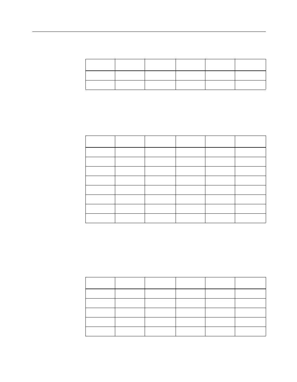
The following table lists the names and positions of the SW1 and SW2
switches for configuring the XC3020A FPGA from the serial PROM
(multiple program).
SW1–7 MCLK OFF SW2–7 RST X
SW1–8 DOUT OFF SW2–8 INIT OFF
X indicates don’t care
Table 3-11 Configuring the XC4003E from the Serial PROM
(Single Program)
Switch Name Position Switch Name Position
SW1–1 INP X SW2–1 PWR X
SW1–2 MPE X SW2–2 MPE OFF
SW1–3 SPE X SW2–3 SPE ON
SW1–4 M0 X SW2–4 M0 OFF
SW1–5 M1 X SW2–5 M1 OFF
SW1–6 M2 X SW2–6 M2 OFF
SW1–7 MCLK OFF SW2–7 RST X
SW1–8 DOUT OFF SW2–8 INIT OFF
X indicates don‘t care
Table 3-12 Configuring the XC3020A from the Serial PROM
(Multiple Program)
Switch Name Position Switch Name Position
SW1–1 INP X SW2–1 PWR X
SW1–2 MPE ON SW2–2 MPE X
SW1–3 SPE OFF SW2–3 SPE X
SW1–4 M0 OFF SW2–4 M0 X
SW1–5 M1 OFF SW2–5 M1 X
Table 3-10 Configuring the XC3020A from the Serial PROM
(Single Program)
Switch Name Position Switch Name Position