42 www.xilinx.com VC709 Evaluation Board
UG887 (v1.0) February 4, 2013
Chapter 1: VC709 Evaluation Board Features
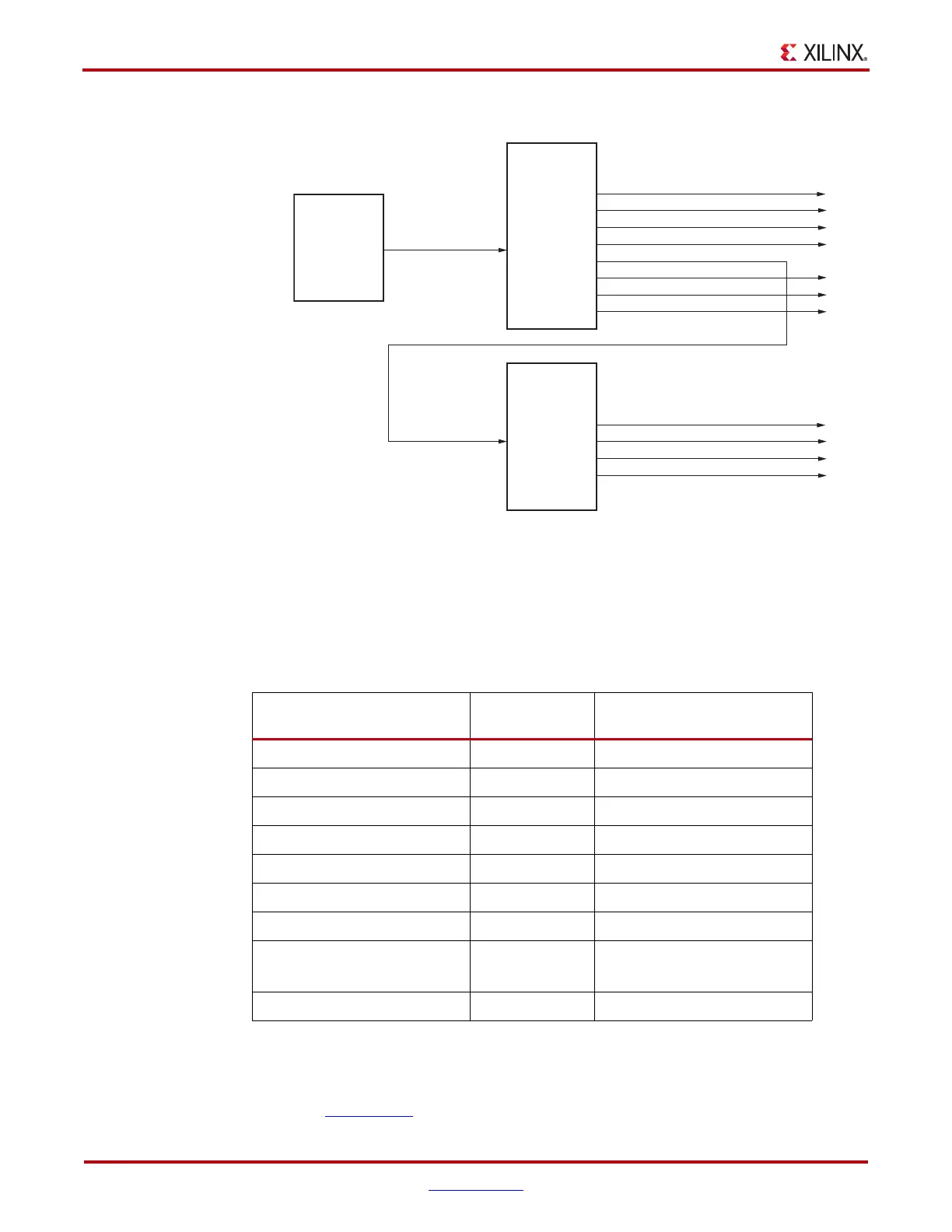
User applications that communicate with devices on one of the downstream I
2
C buses
must first set up a path to the desired bus through the U52 bus switch at I
2
C address 0x74
(0b1110100). Table 1-17 lists the address for each bus. The secondary (SFP+ access) bus
switch U14 is at I²C address 0x75 (0b1110101) and the SFP+ modules all have the same
address 0x50 (0b1010000).
Information about the PCA9546A and PCA9548A is available on the TI Semiconductor
website at www.ti.com
.
X-Ref Target - Figure 1-16
Figure 1-16: I
2
C Bus Topology
Table 1-17: I
2
C Bus Addresses
I
2
C Bus
I
2
C Switch
Position
I
2
C Address
PCA9548 NA 0b1110100
USER_CLK_SDL/SCL 0 0b1011101
FMC1_HPC_IIC_SDA/SCL 1 0bxxxxx00
NOT USED 2 NOT USED
EEPROM_IIC_SDA/SCL 3 0b1010100
PCA9546 (SFP1–SFP4) 4 0b1110101
NOT USED 5 NOT USED
IIC_SDA/SCL_DDR3 J1
IIC_SDA/SCL_DDR3 J3
6
0b1010001, 0b0011001
0b1010010, 0b0011010
Si5324_SDA/SCL 7 0b1101000
Notes:
1. Use the PCA9548 (U52) at I
2
C address 0x74 (0b01110100) to set up the path to these buses.
PCA9548
1
2
C 1-to-8
Bus Switch
CH7 - SI5324_SDA/SCL
0x74
0x75
U52
IIC_SDA/SCL_MAIN
SFP_IIC_SDA/SCL
CH6 - IIC_SDA/SCL_DDR3
CH5 - Not used
CH4 - SFP_IIC_SDA/SCL
CH3 - EEPROM_IIC_SDA/SCL
CH2 - Not used
CH1 - FMC1_HPC_IIC_SDA/SCL
CH0 - USER_CLK_SDL/SCL
FPGA
Bank 15
(2.5V)
U1
PCA9546
1
2
C 1-to-4
Bus Switch
U14
CH0 -SFP1_IIC_SDA/SCL
CH1 -SFP2_IIC_SDA/SCL
CH2 -SFP3_IIC_SDA/SCL
CH3 -SFP4_IIC_SDA/SCL
UG887_c1_16_090612