46 www.xilinx.com VC709 Evaluation Board
UG887 (v1.0) February 4, 2013
Chapter 1: VC709 Evaluation Board Features
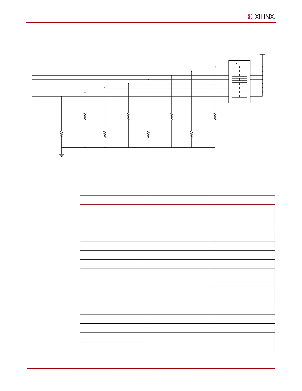
Figure 1-19 shows the GPIO DIP switch circuit.
Table 1-19 lists the GPIO connections to FPGA U1.
X-Ref Target - Figure 1-19
Figure 1-19: GPIO DIP Switch
GPIO_DIP_SW0
GPIO_DIP_SW1
GPIO_DIP_SW2
GPIO_DIP_SW3
GPIO_DIP_SW4
GPIO_DIP_SW5
GPIO_DIP_SW6
GPIO_DIP_SW7
1
2
3
4
5
6
7
8
SW2
SDA08H1SBD
VCC1V8
16
15
14
13
12
11
10
9
2
1
R46
4.7K
1/10W
5%
2
1
R48
4.7K
1/10W
5%
2
1
R53
4.7K
1/10W
5%
2
1
R51
4.7K
1/10W
5%
2
1
R50
4.7K
1/10W
5%
2
1
R52
4.7K
1/10W
5%
2
1
R49
4.7K
1/10W
5%
2
1
R47
4.7K
1/10W
5%
GND
UG887_c1_19_011013
Table 1-19: GPIO Connections to FPGA U1
FPGA (U1) Pin Schematic Net Name GPIO Pin
Indicator LEDs (Active-High)
AM39 GPIO_LED_0 DS2.2
AN39 GPIO_LED_1 DS3.2
AR37 GPIO_LED_2 DS4.2
AT37 GPIO_LED_3 DS5.2
AR35 GPIO_LED_4 DS6.2
AP41 GPIO_LED_5 DS7.2
AP42 GPIO_LED_6 DS8.2
AU39GPIO_LED_7DS9.2
Directional Pushbutton Switches
AR40 GPIO_SW_N SW3.3
AU38 GPIO_SW_E SW4.3
AP40 GPIO_SW_S SW5.3
AW40 GPIO_SW_W SW7.3
AV39 GPIO_SW_C SW6.3
8-Pole DIP Switch