Embedded Tri-Mode Ethernet MAC User Guide www.xilinx.com 79
UG074 (v2.2) February 22, 2010
Host Interface
R
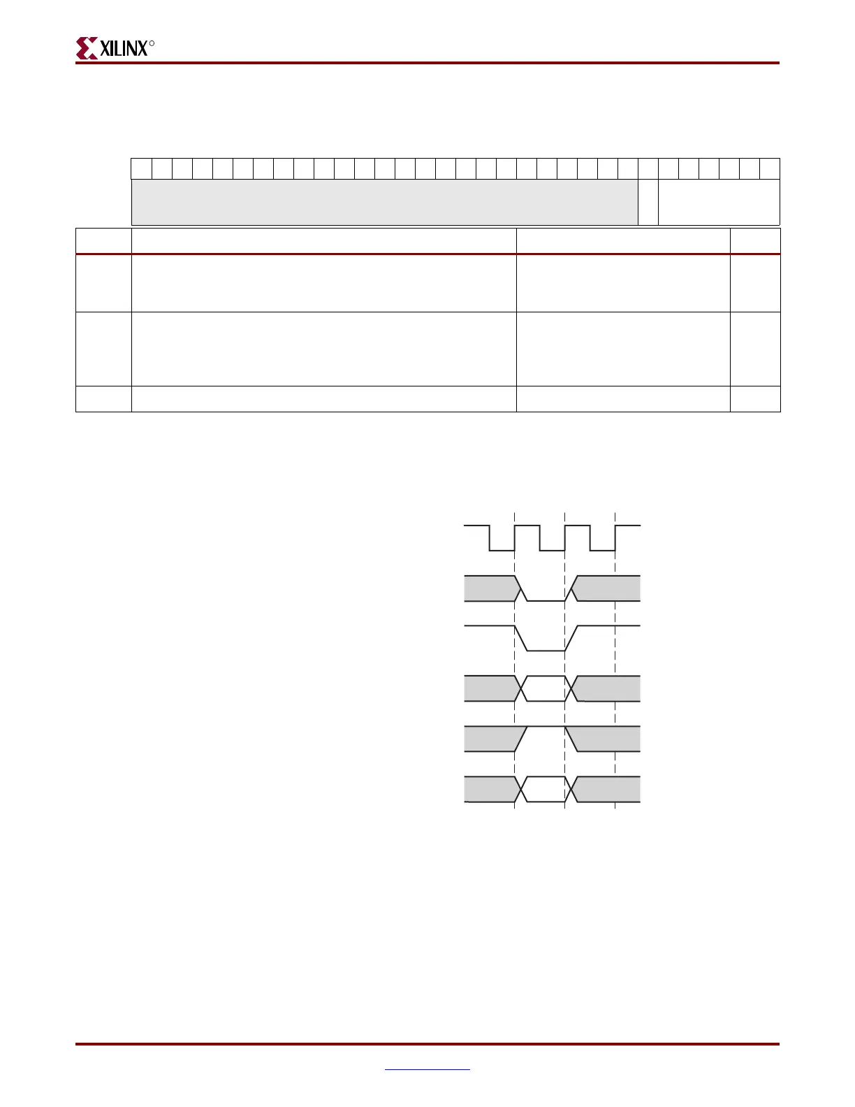
Figure 3-40 shows the write timing for the configuration registers through the
management interface. When accessing the configuration registers (i.e., when
HOSTADDR[9] = 1 and HOSTMIIMSEL = 0), the upper bit of HOSTOPCODE functions as
an active Low write-enable signal. The lower HOSTOPCODE bit (bit[0]) is a “don’t care.”
Table 3-14: Management Configuration Register
MSB
LSB
313029282726252423222120191817161514131211109876543210
0x340
RESERVED
MDIOEN
CLOCK_DIVIDE[5:0]
Bit Description Default Value R/W
[5:0]
Clock divide [5:0]: This value is used to derive the
EMAC#PHYMCLKOUT for external devices.
See “MDIO Interface,” page 93.
All 0sR/W
[6]
MDIO enable: When this bit is 1, the MDIO interface is used to
access the PHY. When this bit is 0, the MDIO interface is
disabled, and the MDIO signals remain inactive.
See “MDIO Interface,” page 93.
TIEEMAC#CONFIGVEC[73] R/W
[31:7] Reserved. –
Figure 3-40: Configuration Register Write Timing
HOSTCLK
HOSTADDR[8:0]
HOSTADDR[9]
HOSTOPCODE[1]
HOSTMIIMSEL
HOSTWRDATA[31:0]
ug074_3_42_080805