4. Interfacing to the world 55
4.3.2.4 5 to 24 V Output
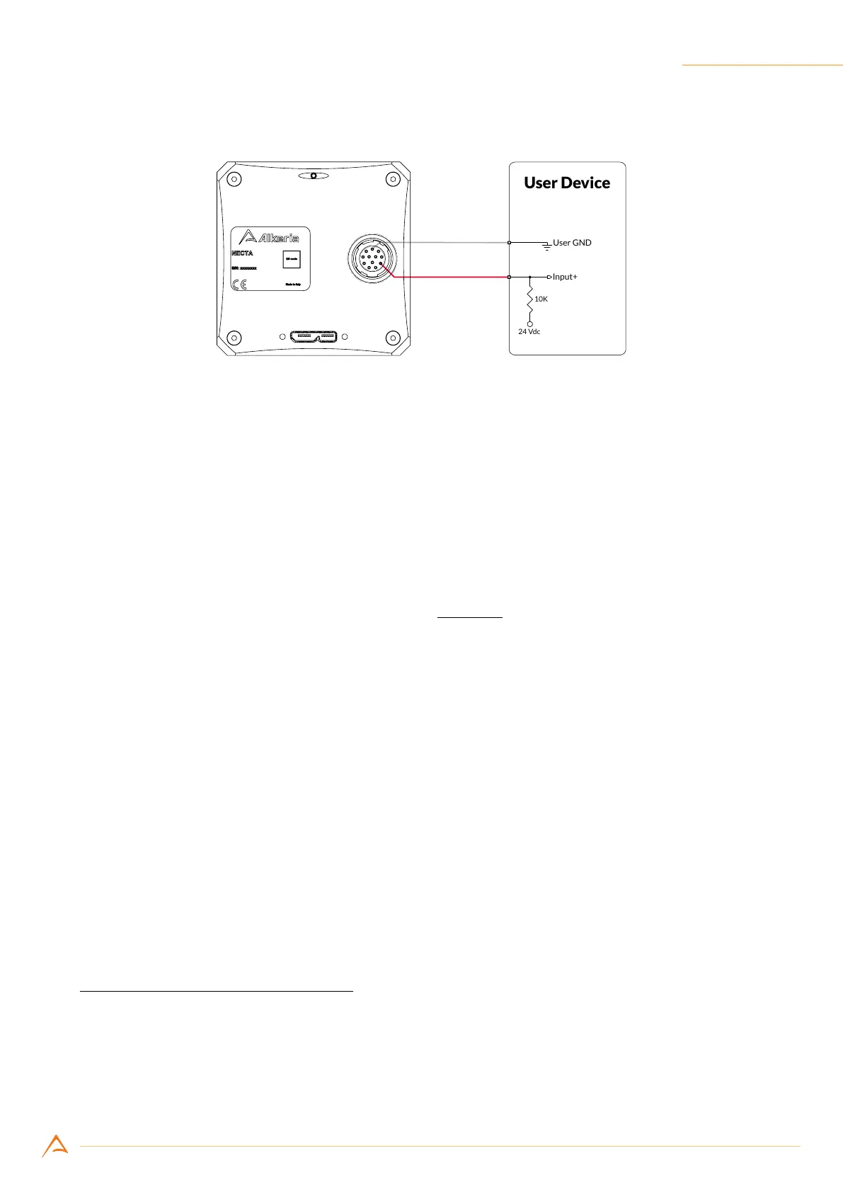
Figure 4.16: Connecting output port P3+ to a 24 V input
NECTA with 24 V tolerant I/O interface can drive also 5 to 24 V inputs using the connections shown in
Figure 4.16: the ‘0’ logic level is generate by the output driver ”shorting” the external pullup resistor
to ground, while the ‘1’ level is imposed by the external pullup voltage. This conguration needs to be
enabled using the procedure in Section 4.5.2.
External pullup resistor value must be calculate in order to maintain the 0 V output current under 30 mA,
as shown below:
R
P ullup
[kΩ] ≥
V
P ullup
[V]
30 mA
(4.1)
Note that the lowest pullup value, the slowest commutation time, the highest ’0’ logic voltage value.
4.3.3 Bidirectional module structure (port 0)
NECTA port 0 can be software-congured either as an input or as an output. When the camera is pow-
ered on, the port is initially congured as an input (termination disabled); it can be set as an output by
software. All the statements above about input and output ports, including methods to interface to
signals with logic levels different from RS-422, apply also to port 0. For more information on how to
congure and use the input/output port refer to the code samples in Section 4.5 and to the examples
found in the MaestroUSB3 SDK.
4.3.4 I/O switching time
As reported in the I/O schematics shown in Figure 4.4-4.5 and below, NECTA cameras use RS-422 differ-
ential transceivers mod. LTC2855-LTC2865, made by Linear Technology. They allow very short switch-
ing time: the input propagation delay, due to the input receiver, is less than 70 ns, the output delay is
less than 50 ns
1
; both rise and fall time are less than 12.5 ns.
1
Valid only for push-pull output congurations. When the output is open-collector, delay depends on the external pull-up.