4. Interfacing to the world 54
Warning
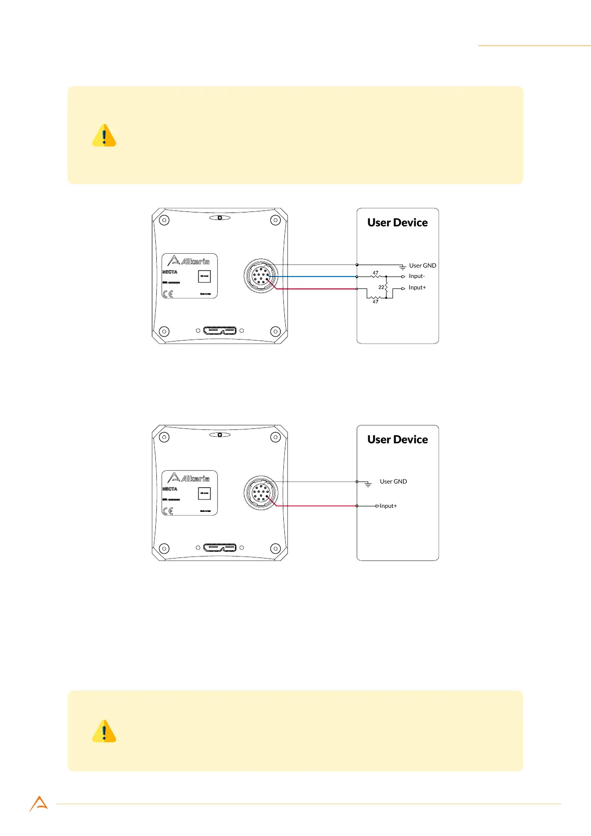
Connecting NECTA camera outputs to an external RS-644 device inputs
WITHOUT using the recommended resistive divider may seriously damage
your device.
Figure 4.14: Connecting output port P3 to a RS-644 input
4.3.2.3 LV-TTL / LV-CMOS
Figure 4.15: Connecting output port P3+ to a LV-TTL / LV-CMOS input
NECTA outputs can be interfaced also to LV-TTL/LV-CMOS inputs using the connections shown in Fig-
ure 4.15: the ‘0’ logic level generated by the output driver is lower than 0.5 V, while the ‘1’ level is about
3.3 V; both levels therefore satisfy the input requirements for both LV-TTL and LV-CMOS signaling.
Please connect the P+ output for direct signaling, or P- output for inverted logic signaling.
Warning
To ensure proper operation of the output circuit, the camera reference ground
must be connected to the slave device as well.