Host Interface 25 (114)
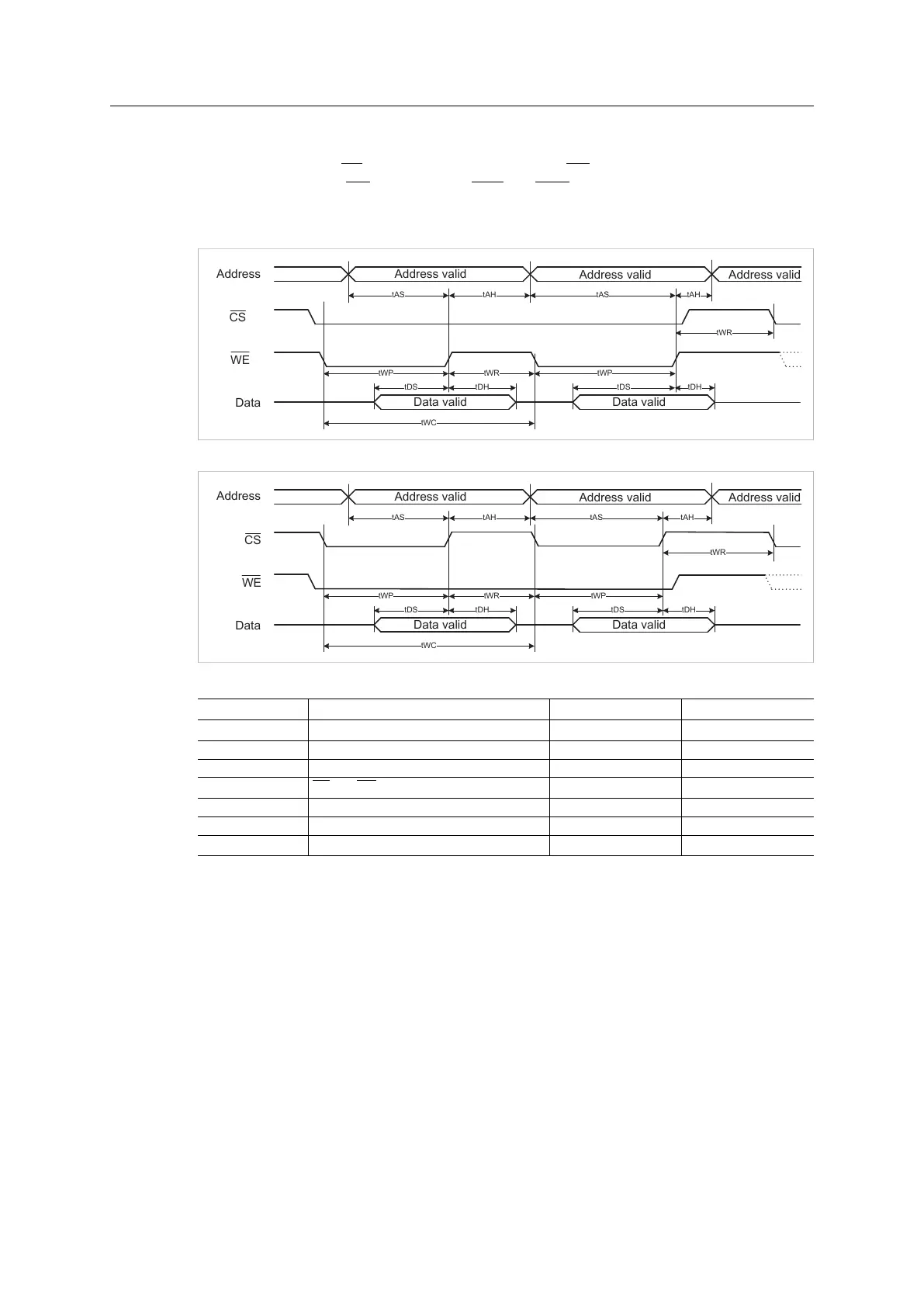
3.3.5 Memory Access Write Timing
It doesn’t matter if the OE signal is low or high as long as WE is active (low). In 16 bit mode, the
timing requirements of WE applies to both WEL and WEH. The timing diagrams show a burst
write but the timing applies for a single write as well. The first diagram shows write enable
controlled write timing and the second shows chip select controlled write timing.
Address
CS
WE
Data
Data valid
Data valid
tAS tAH
tWP
Address valid
Address valid
tDHtDS
tWR
tAS tAH
tWP
tDHtDS
tWC
tWR
Address valid
Fig. 8
Address
CS
WE
Data
Data valid
Data valid
tAS tAH
tWP
Address valid
Address valid
tDHtDS
tWR
tAS tAH
tWP
tDHtDS
tWC
tWR
Address valid
Fig. 9
Symbol Parameter Min (ns) Max (ns)
tWC Write cycle time 30
-
tAS Address valid before End-of-Write 15
-
tAH Address valid after End-of-Write 0
-
tWP CS and WE low pulse width 15
-
tDS Data valid before End-of-Write 15
-
tDH Data valid after End-of-Write 0
-
tWR Write recovery time 10
-
Anybus
®
CompactCom
™
M40 Hardware Design Guide HMSI-216-126 EN 2.6