BURN BACK
1
2
3
4
5
6
7
8
CN6
8
9
11
10
6
7
16
15
C41
103
D30
1N4007
VCC
U7
P521
R12
2k4
VCC
1 2
147
U8A
14584
3 4
U8B
14584
C42
104
VCC
C17
104
R11
820R
R19
56K
5
6
7
U1B
LM358
R75
10K
R76
10K
VCC
R77
1K
C43
104
22A
27
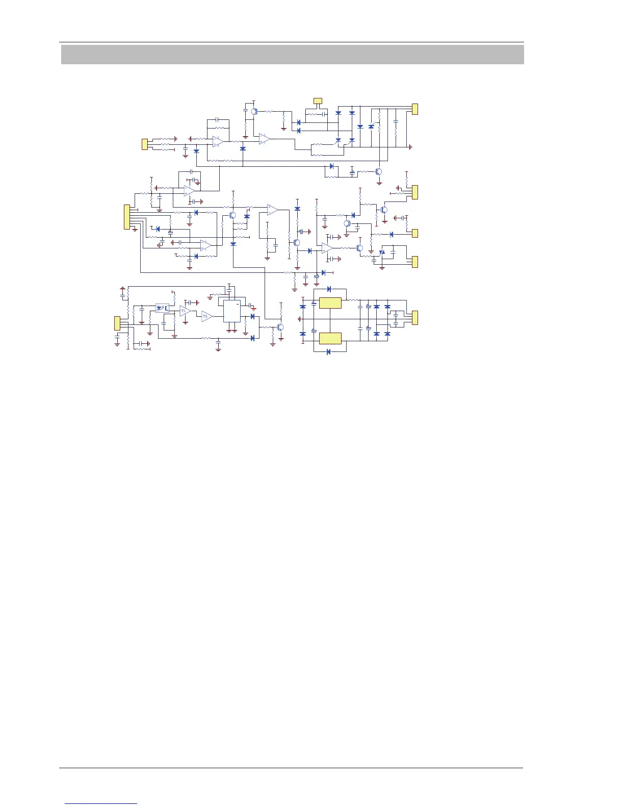
Art # A-10150
Figure 1 – Circuit Diagram Control PCB for Weldskill 250 & 350
2. Power Supply
40 VAC CT is derived from the auxiliary transformer.
This AC voltage is full wave rectified by diodes D6, D7, D8, D9 and the resultant DC voltage is smoothed by
C11 & C12 to provide a low ripple DC supply of approximately 28V. This voltage is regulated to +/- 15V by
regulators W1 & W2 and smoothed by capacitors C19 & C20.
3. Standby (Torch trigger switch open)
Transistor Q8 input is held to ground by R39. The collector of Q8 is held high by R38. D20 is reverse biased,
and Q7 is off.
The collector of Q7 is high, so U5a pin 2 is held above pin 3, and the output pin 1 is low, disabling the motor
control via D28 & D29.
In SPOT mode or 2T mode, the switch connected to CN7 terminals 1 & 2 will be closed. This pulls U2 pin 4
high through R71, R72, & R73, forcing U2 pin 1 to be low.
4. Torch trigger switch closed
When the torch trigger switch is closed, +15V feeds through R59, R60 & R53 to turn on Q8. The collector of
Q8 goes low, pulling the emitter of Q7 low. This pulls the collector low causing U5 pin 2 to fall below pin 3,
and causing pin 1 to go high. D28 & D29 are now reverse biased allowing U5 pin 8 to send phase angle control
pulses to SCR’s U3 & U4. The collector of Q7 which is now low, causes U1 pin 5 to fall below pin 6, and the
output pin 7 goes low, turning on Q3 which causes U1 pin 3 to go high, and charges C6. U1 pin 1 goes high
turning on Q2, which turns on Q1, engaging the contactor and enabling welding output.
When the torch trigger switch is closed, U7 is turned on via R51 & R12. The output of U7 will be closed and
U8 pin 1 will be high. U8 pin 4 will also be high putting a positive going clock signal into U2. The output of
U2, pin 1,remains low as U2 pin 4 is being held high in SPOT or 2T mode.