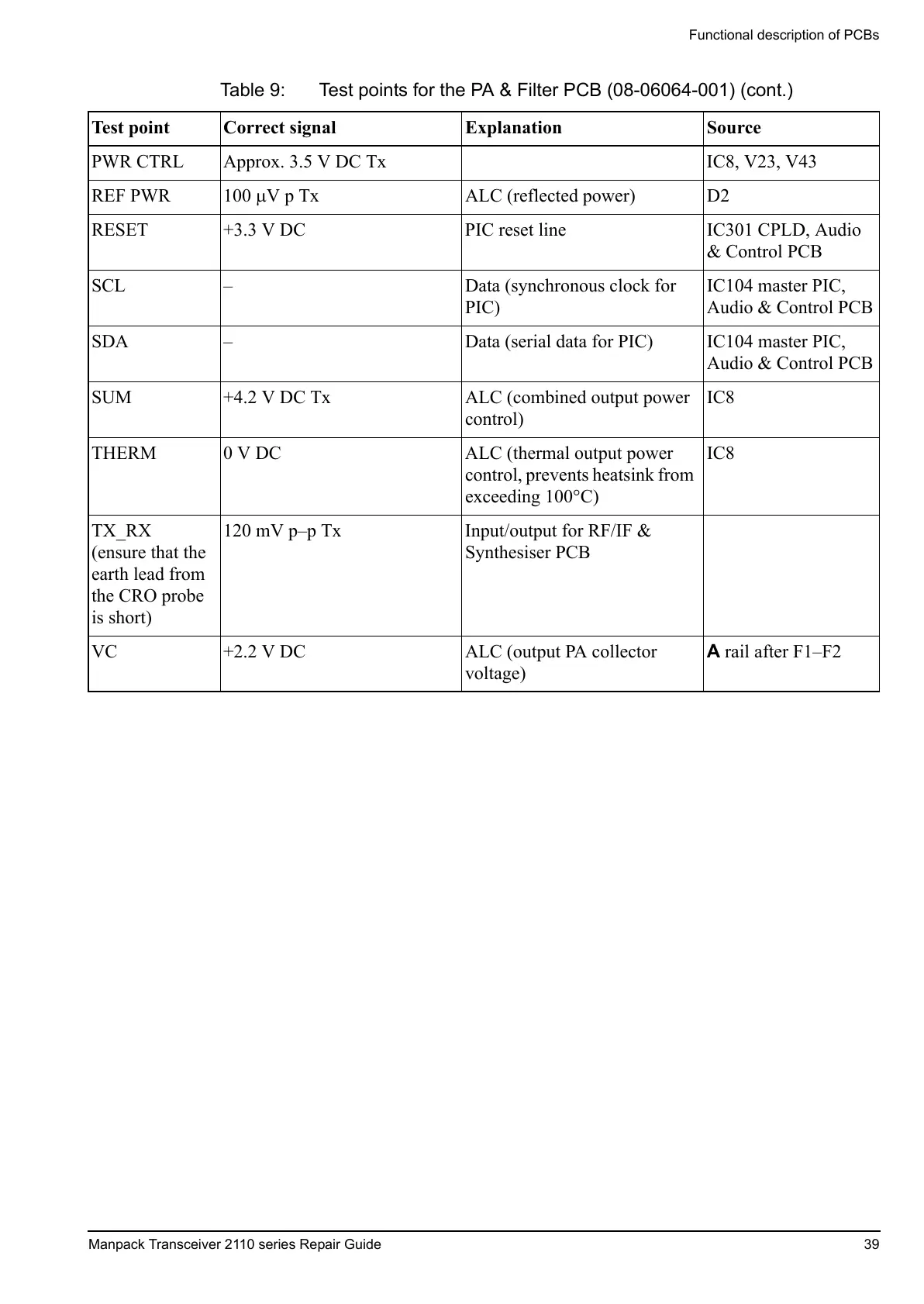
Functional description of PCBs
Manpack Transceiver 2110 series Repair Guide 39
PWR CTRL Approx. 3.5 V DC Tx IC8, V23, V43
REF PWR 100 V p Tx ALC (reflected power) D2
RESET +3.3 V DC PIC reset line IC301 CPLD, Audio
& Control PCB
SCL – Data (synchronous clock for
PIC)
IC104 master PIC,
Audio & Control PCB
SDA – Data (serial data for PIC) IC104 master PIC,
Audio & Control PCB
SUM +4.2 V DC Tx ALC (combined output power
control)
IC8
THERM 0 V DC ALC (thermal output power
control, prevents heatsink from
exceeding 100°C)
IC8
TX_RX
(ensure that the
earth lead from
the CRO probe
is short)
120 mV p–p Tx Input/output for RF/IF &
Synthesiser PCB
VC +2.2 V DC ALC (output PA collector
voltage)
A rail after F1–F2
Table 9: Test points for the PA & Filter PCB (08-06064-001) (cont.)
Test point Correct signal Explanation Source
 Loading...