Functional description of PCBs
34 Manpack Transceiver 2110 series Repair Guide
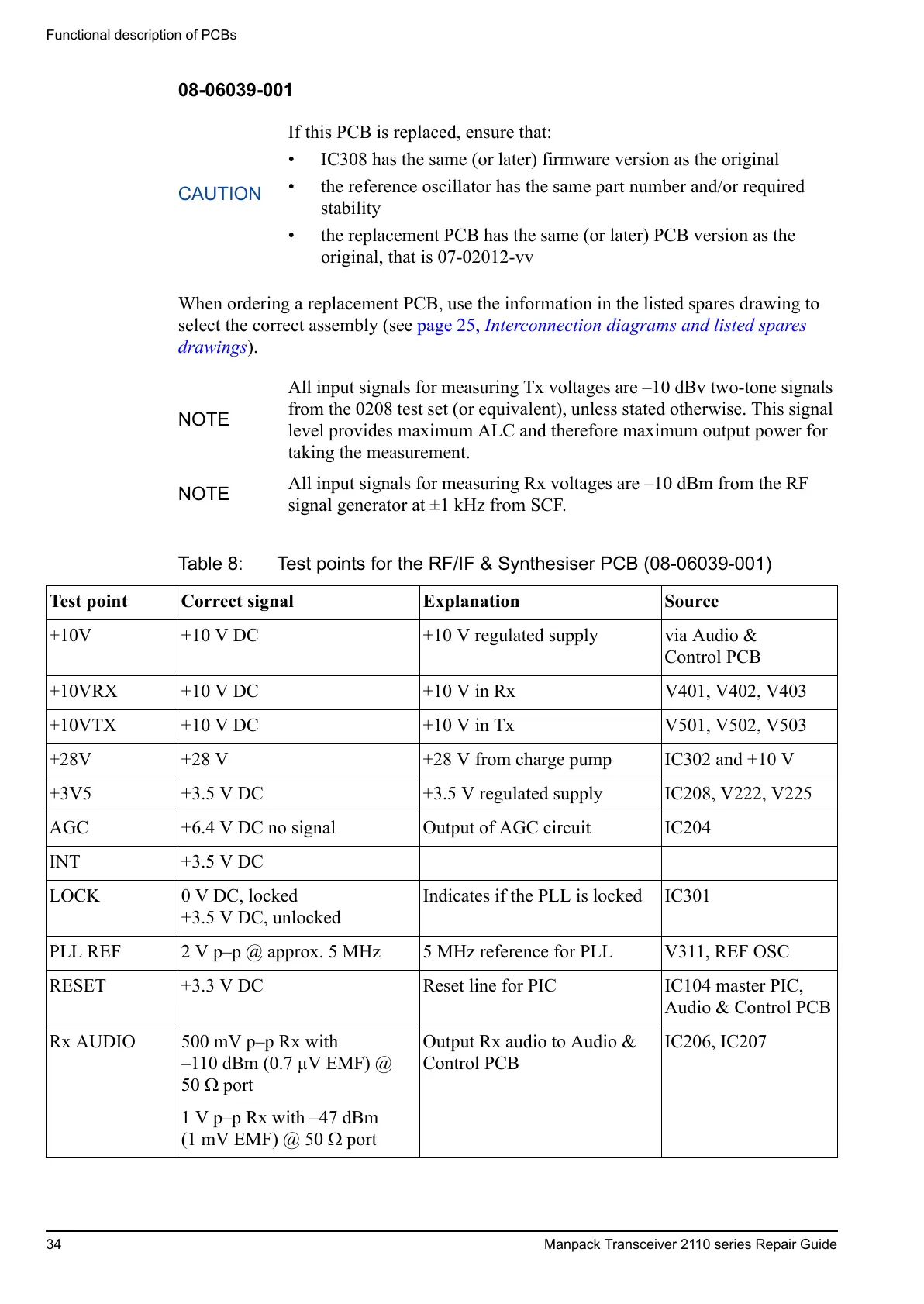
08-06039-001
When ordering a replacement PCB, use the information in the listed spares drawing to
select the correct assembly (see page 25, Interconnection diagrams and listed spares
drawings).
CAUTION
If this PCB is replaced, ensure that:
• IC308 has the same (or later) firmware version as the original
• the reference oscillator has the same part number and/or required
stability
• the replacement PCB has the same (or later) PCB version as the
original, that is 07-02012-vv
NOTE
All input signals for measuring Tx voltages are –10 dBv two-tone signals
from the 0208 test set (or equivalent), unless stated otherwise. This signal
level provides maximum ALC and therefore maximum output power for
taking the measurement.
NOTE
All input signals for measuring Rx voltages are –10 dBm from the RF
signal generator at ±1 kHz from SCF.
Table 8: Test points for the RF/IF & Synthesiser PCB (08-06039-001)
Test point Correct signal Explanation Source
+10V +10 V DC +10 V regulated supply via Audio &
Control PCB
+10VRX +10 V DC +10 V in Rx V401, V402, V403
+10VTX +10 V DC +10 V in Tx V501, V502, V503
+28V +28 V +28 V from charge pump IC302 and +10 V
+3V5 +3.5 V DC +3.5 V regulated supply IC208, V222, V225
AGC +6.4 V DC no signal Output of AGC circuit IC204
INT +3.5 V DC
LOCK 0 V DC, locked
+3.5 V DC, unlocked
Indicates if the PLL is locked IC301
PLL REF 2 V p–p @ approx. 5 MHz 5 MHz reference for PLL V311, REF OSC
RESET +3.3 V DC Reset line for PIC IC104 master PIC,
Audio & Control PCB
Rx AUDIO 500 mV p–p Rx with
–110 dBm (0.7 µV EMF) @
50 port
1 V p–p Rx with –47 dBm
(1 mV EMF) @ 50 port
Output Rx audio to Audio &
Control PCB
IC206, IC207
 Loading...