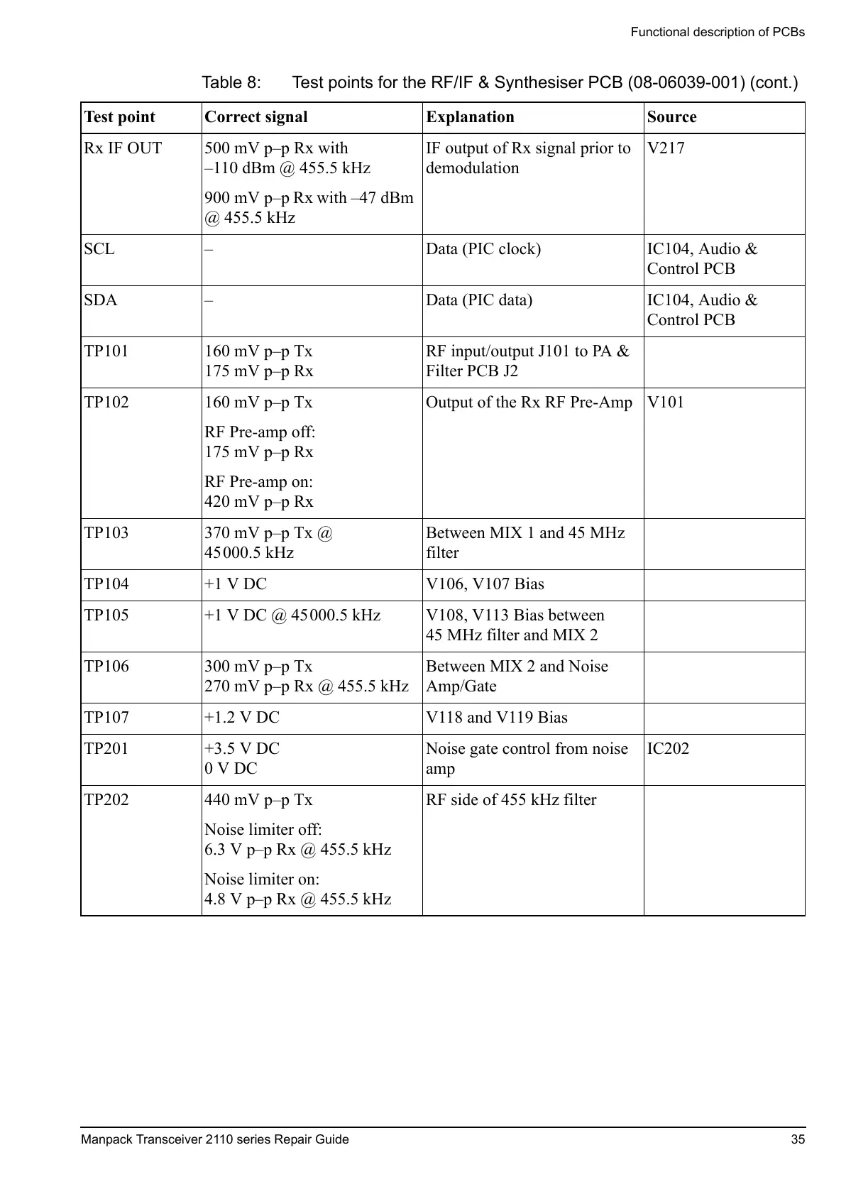
Functional description of PCBs
Manpack Transceiver 2110 series Repair Guide 35
Rx IF OUT 500 mV p–p Rx with
–110 dBm @ 455.5 kHz
900 mV p–p Rx with –47 dBm
@ 455.5 kHz
IF output of Rx signal prior to
demodulation
V217
SCL – Data (PIC clock) IC104, Audio &
Control PCB
SDA – Data (PIC data) IC104, Audio &
Control PCB
TP101 160 mV p–p Tx
175 mV p–p Rx
RF input/output J101 to PA &
Filter PCB J2
TP102 160 mV p–p Tx
RF Pre-amp off:
175 mV p–p Rx
RF Pre-amp on:
420 mV p–p Rx
Output of the Rx RF Pre-Amp V101
TP103 370 mV p–p Tx @
45000.5 kHz
Between MIX 1 and 45 MHz
filter
TP104 +1 V DC V106, V107 Bias
TP105 +1 V DC @ 45000.5 kHz V108, V113 Bias between
45 MHz filter and MIX 2
TP106 300 mV p–p Tx
270 mV p–p Rx @ 455.5 kHz
Between MIX 2 and Noise
Amp/Gate
TP107 +1.2 V DC V118 and V119 Bias
TP201 +3.5 V DC
0VDC
Noise gate control from noise
amp
IC202
TP202 440 mV p–p Tx
Noise limiter off:
6.3 V p–p Rx @ 455.5 kHz
Noise limiter on:
4.8 V p–p Rx @ 455.5 kHz
RF side of 455 kHz filter
Table 8: Test points for the RF/IF & Synthesiser PCB (08-06039-001) (cont.)
Test point Correct signal Explanation Source
 Loading...