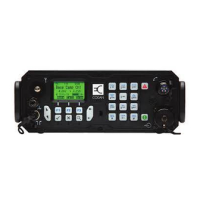
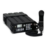
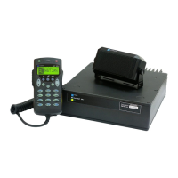
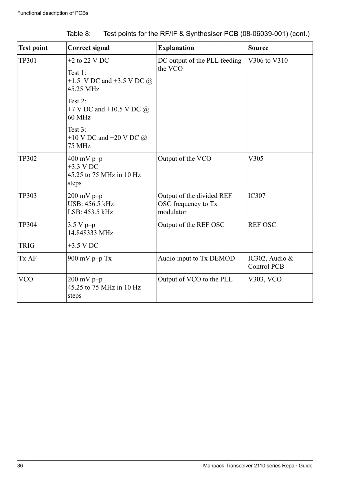
Functional description of PCBs
36 Manpack Transceiver 2110 series Repair Guide
TP301 +2 to 22 V DC
Test 1:
+1.5 V DC and +3.5 V DC @
45.25 MHz
Test 2:
+7 V DC and +10.5 V DC @
60 MHz
Test 3:
+10 V DC and +20 V DC @
75 MHz
DC output of the PLL feeding
the VCO
V306 to V310
TP302 400 mV p–p
+3.3 V DC
45.25 to 75 MHz in 10 Hz
steps
Output of the VCO V305
TP303 200 mV p–p
USB: 456.5 kHz
LSB: 453.5 kHz
Output of the divided REF
OSC frequency to Tx
modulator
IC307
TP304 3.5 V p–p
14.848333 MHz
Output of the REF OSC REF OSC
TRIG +3.5 V DC
Tx AF 900 mV p–p Tx Audio input to Tx DEMOD IC302, Audio &
Control PCB
VCO 200 mV p–p
45.25 to 75 MHz in 10 Hz
steps
Output of VCO to the PLL V303, VCO
Table 8: Test points for the RF/IF & Synthesiser PCB (08-06039-001) (cont.)
Test point Correct signal Explanation Source
 Loading...