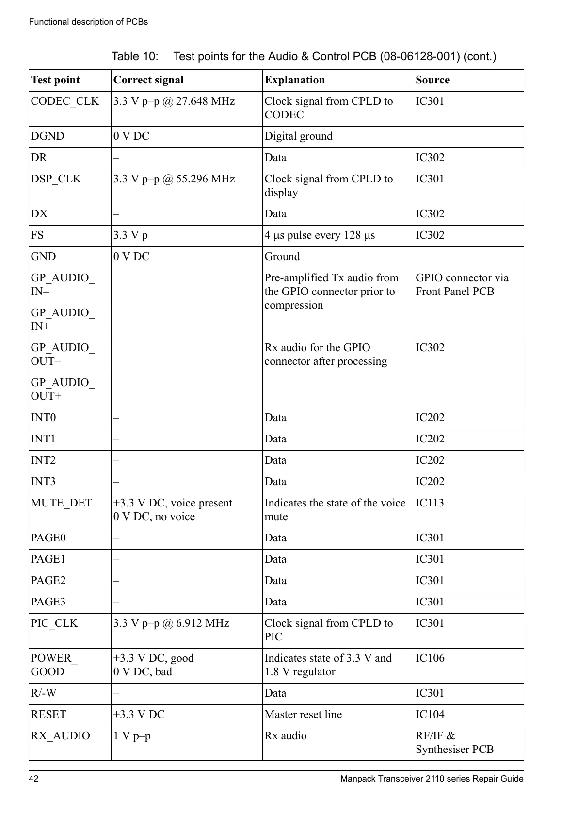
Functional description of PCBs
42 Manpack Transceiver 2110 series Repair Guide
CODEC_CLK 3.3 V p–p @ 27.648 MHz Clock signal from CPLD to
CODEC
IC301
DGND 0 V DC Digital ground
DR – Data IC302
DSP_CLK 3.3 V p–p @ 55.296 MHz Clock signal from CPLD to
display
IC301
DX – Data IC302
FS 3.3 V p 4 s pulse every 128 s IC302
GND 0 V DC Ground
GP_AUDIO_
IN–
Pre-amplified Tx audio from
the GPIO connector prior to
compression
GPIO connector via
Front Panel PCB
GP_AUDIO_
IN+
GP_AUDIO_
OUT–
Rx audio for the GPIO
connector after processing
IC302
GP_AUDIO_
OUT+
INT0 – Data IC202
INT1 – Data IC202
INT2 – Data IC202
INT3 – Data IC202
MUTE_DET +3.3 V DC, voice present
0 V DC, no voice
Indicates the state of the voice
mute
IC113
PAGE0 – Data IC301
PAGE1 – Data IC301
PAGE2 – Data IC301
PAGE3 – Data IC301
PIC_CLK 3.3 V p–p @ 6.912 MHz Clock signal from CPLD to
PIC
IC301
POWER_
GOOD
+3.3 V DC, good
0 V DC, bad
Indicates state of 3.3 V and
1.8 V regulator
IC106
R/-W – Data IC301
RESET +3.3 V DC Master reset line IC104
RX_AUDIO 1 V p–p Rx audio RF/IF &
Synthesiser PCB
Table 10: Test points for the Audio & Control PCB (08-06128-001) (cont.)
Test point Correct signal Explanation Source
 Loading...