Functional description of PCBs
Manpack Transceiver 2110 series Repair Guide 49
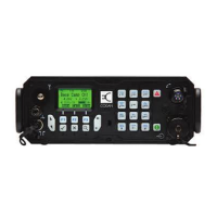
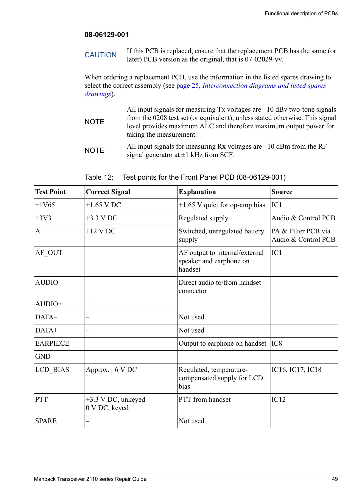
08-06129-001
When ordering a replacement PCB, use the information in the listed spares drawing to
select the correct assembly (see page 25, Interconnection diagrams and listed spares
drawings).
CAUTION
If this PCB is replaced, ensure that the replacement PCB has the same (or
later) PCB version as the original, that is 07-02029-vv.
NOTE
All input signals for measuring Tx voltages are –10 dBv two-tone signals
from the 0208 test set (or equivalent), unless stated otherwise. This signal
level provides maximum ALC and therefore maximum output power for
taking the measurement.
NOTE
All input signals for measuring Rx voltages are –10 dBm from the RF
signal generator at ±1 kHz from SCF.
Table 12: Test points for the Front Panel PCB (08-06129-001)
Test Point Correct Signal Explanation Source
+1V65 +1.65 V DC +1.65 V quiet for op-amp bias IC1
+3V3 +3.3 V DC Regulated supply Audio & Control PCB
A +12 V DC Switched, unregulated battery
supply
PA & Filter PCB via
Audio & Control PCB
AF_OUT AF output to internal/external
speaker and earphone on
handset
IC1
AUDIO– Direct audio to/from handset
connector
AUDIO+
DATA– – Not used
DATA+ – Not used
EARPIECE Output to earphone on handset IC8
GND
LCD_BIAS Approx. –6 V DC Regulated, temperature-
compensated supply for LCD
bias
IC16, IC17, IC18
PTT +3.3 V DC, unkeyed
0 V DC, keyed
PTT from handset IC12
SPARE – Not used
 Loading...