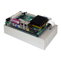
DIGITAL-LOGIC AG PCCP5 Manual V2.3
80
Definition of CHIPSMM.H
/************************************************************************
* Description: Hardware register definitiona file for 6555x *
* Copyright (C) Chips and Technologies, Inc. 1995 *
************************************************************************/
#define WritePortUchar(p,v) outp((USHORT)p,v)
#define WritePortUshort(p,v) outpw((USHORT)p,v)
#define WritePortUlong(p,v) outpd((USHORT)p,v)
#define ReadPortUchar(p) inp((USHORT)p)
#define ReadPortUshort(p) inpw((USHORT)p)
#define ReadPortUlong(p) inpd((USHORT)p)
//------------------------------------------------------------------------
// Chips multimedia register description for 6555x registers.
// Any chages here must also be made in CHIPSMMH.INC
//------------------------------------------------------------------------
#define ADDR_FR 0x03d0 // C&T Flat Panel Register address port
#define DATA_FR 0x03d1 // C&T Flat Panel Register data port
#define ADDR_MR 0x03d2 // C&T Multimedia Register address port
#define DATA_MR 0x03d3 // C&T Multimedia Register data port
#define ADDR_EXTR 0x03d6 // C&T XR Address
#define DATA_EXTR 0x03d7 // C&T XR Data
#define MR_CAPS_REG_1 0x00 // Multimedia capabilities reg 1
#define MR_CAPS_REG_2 0x01 // Multimedia capabilities reg 2
#define MR_VIN_CTRL_1 0x02 // Video Input Control Reg 1
#define MR_VIN_CTRL_2 0x03 // Video Input Control Reg 2
#define MR_VIN_CTRL_3 0x04 // Video Input Control Reg 3
#define MR_VIN_CTRL_4 0x05 // Video Input Control Reg 4(stat reg)
#define MR_VIN_ADDR_1_L 0x06 // Video Input Address Pointer 1 (low)
#define MR_VIN_ADDR_1_M 0x07 // Video Input Address Pointer 1 (mid)
#define MR_VIN_ADDR_1_H 0x08 // Video Input Address Pointer 1 (high)
#define MR_VIN_ADDR_2_L 0x09 // Video Input Address Pointer 2 (low)
#define MR_VIN_ADDR_2_M 0x0A // Video Input Address Pointer 2 (mid)
#define MR_VIN_ADDR_2_H 0x0B // Video Input Address Pointer 2 (high)
#define MR_VIN_PITCH_QD 0x0C // Pitch of Video Input buff in quad
// words (8 bytes = 1QD)
#define MR_VIN_AQW_XL_L 0x0E // Aquisition Window X-Left low
#define MR_VIN_AQW_XL_H 0x0F // Aquisition Window X-Left high
#define MR_VIN_AQW_XR_L 0x10 // Aquisition Window X-Right low
#define MR_VIN_AQW_XR_H 0x11 // Aquisition Window X-Right high
#define MR_VIN_AQW_YT_L 0x12 // Aquisition Window Y-Top low
#define MR_VIN_AQW_YT_H 0x13 // Aquisition Window Y-Top high
#define MR_VIN_AQW_YB_L 0x14 // Aquisition Window Y-Bottom low
#define MR_VIN_AQW_YB_H 0x15 // Aquisition Window Y-Bottom high
#define MR_VIN_SCALE_X 0x16 // Video Input Horizontal scale factor
#define MR_VIN_SCALE_Y 0x17 // Video Input Vertical scale factor
#define MR_VIN_FRMCOUNT 0x18 // Frame Count for Nth Frame capturing
//------------------------------------------------------------------------
// Video Display Registers:
//------------------------------------------------------------------------
#define MR_VDP_CTRL_1 0x1E // Video Display Control Reg 1
#define MR_VDP_CTRL_2 0x1F // Video Display Control Reg 2
#define MR_VDP_CTRL_3 0x20 // Video Display Control Reg 3
#define MR_VDP_CTRL_4 0x21 // Video Display Control Reg 4 (status)
#define MR_VDP_ADDR_1_L 0x22 // Video Display Addr Pointer 1 (low)
#define MR_VDP_ADDR_1_M 0x23 // Video Display Addr Pointer 1 (mid)
#define MR_VDP_ADDR_1_H 0x24 // Video Display Addr Pointer 1 (high)
#define MR_VDP_ADDR_2_L 0x25 // Video Display Addr Pointer 2 (low)
#define MR_VDP_ADDR_2_M 0x26 // Video Display Addr Pointer 2 (mid)
#define MR_VDP_ADDR_2_H 0x27 // Video Display Addr Pointer 2 (high)