2 Module Description
2.1 Block Diagram
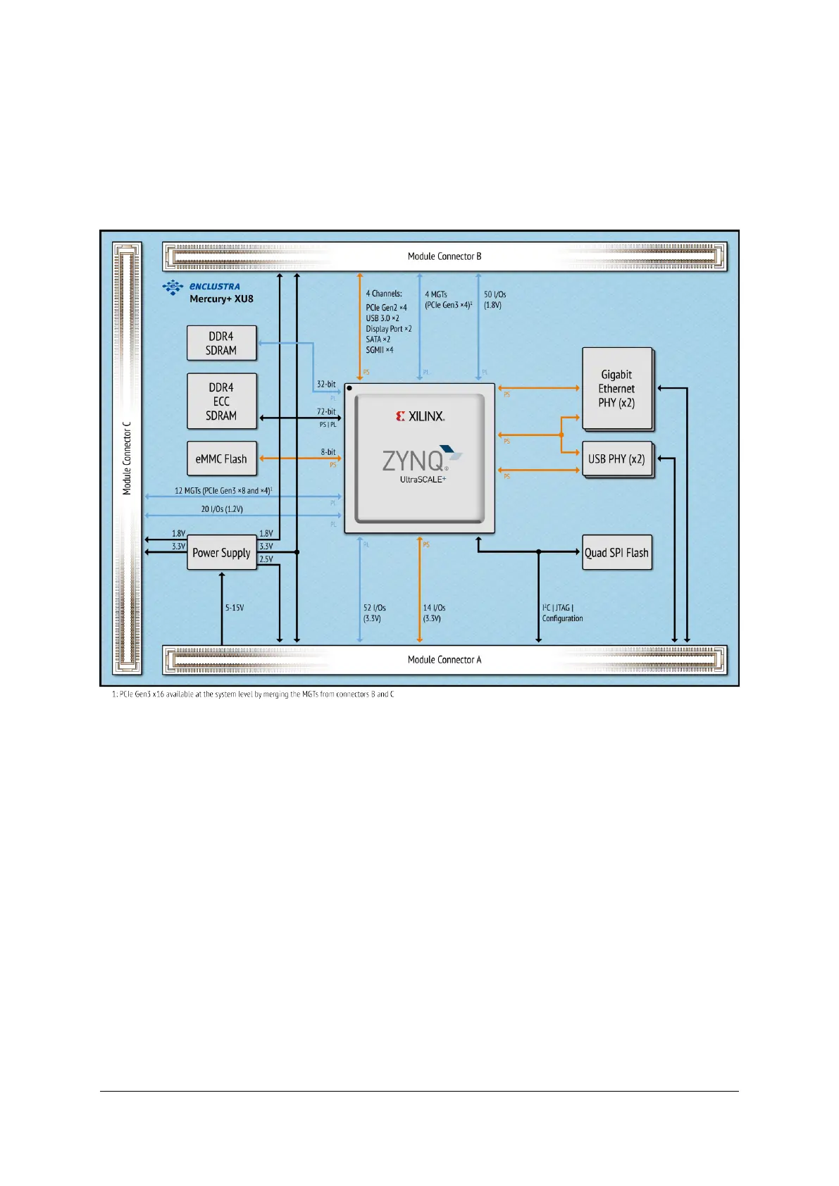
Figure 1: Hardware Block Diagram
The main component of the Mercury+ XU8 SoC module is the Xilinx Zynq Ultrascale+ MPSoC device. Most of
its I/O pins are connected to the Mercury+ module connector, making 136 regular user I/Os available to the
user. Further, twenty MGT pairs are available on the module connector, making possible the implementation
of several high-speed protocols such as PCIe Gen3 ×16, PCIe Gen2 ×4 and USB 3.0 (simultaneous usage of
all the interfaces is limited to the available hardware resources i.e. number of transceivers and lane mapping).
The MPSoC device can boot from the on-board QSPI flash, from the eMMC flash or from an external SD
card. For development purposes, a JTAG interface is connected to Mercury module connector.
The available standard configurations include a 16 GB eMMC flash, a 64 MB quad SPI flash, up to 4 GB DDR4
SDRAM with ECC connected to the Processing System (PS) and up to 2 GB DDR4 SDRAM connected to the
Programmable Logic (PL).
Further, the module is equipped with two Gigabit Ethernet PHYs and two USB 2.0 PHYs, making it ideal for
communication applications.
A real-time clock is available on the Xilinx Zynq Ultrascale+ MPSoC device.
D-0000-454-001 10 / 60 Version 06, 18.11.2019
 Loading...


