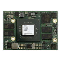
Warning!
Do not use excessive force to latch a Mercury module into the Mercury connectors on the base board,
as this could damage the module and the base board; always make sure that the module is correctly
oriented before mounting it into the base board.
2.9 User I/O
2.9.1 Pinout
Information on the Mercury+ XU8 SoC module pinout can be found in the Enclustra Mercury Master Pinout
[11], and in the additional document Enclustra Module Pin Connection Guidelines [10].
Warning!
Please note that the pin types on the schematics symbol of the module connector and in the Master
Pinout document are for reference only. On the Mercury+ XU8 SoC module it may be possible that
the connected pins do not have the targeted functions (such as primary clocks, differential pins, MGT
signals, etc).
The naming convention for the user I/Os located in HP banks is:
IO_B<BANK>_L<PAIR><_SPECIAL_FUNCTION>_<PACKAGE_PIN>_<POLARITY>.
For example, IO_B66_L4_AD7_AD11_P is located on pin AD11 of I/O bank 66, pair 4, it is a System Monitor
differential auxiliary analog input capable pin and it has positive polarity, when used in a differential pair.
The HD banks are numbered differently depending on the MPSoC device equipped on the module:
• Bank N represents:
• I/O bank 46 for ZU4/ZU5 devices
• I/O bank 47 for ZU7 devices
• Bank O represents:
• I/O bank 45 for ZU4/ZU5 devices
• I/O bank 48 for ZU7 devices
The naming convention for the user I/Os located in HD banks is:
IO_B<BANK_LETTER>_L<PAIR><_SPECIAL_FUNCTION>_<PACKAGE_PIN>_<POLARITY>
For example, IO_BN_L7_HDGC_AD5_E13_N is located on pin E13 of I/O bank N, pair 7, it is a System Monitor
differential auxiliary analog input capable pin and also a clock capable pin and it has negative polarity, when
used in a differential pair.
The global clock capable pins are marked with “GC” (HP I/O banks) or with “HDGC” (HD I/O banks) in the
signal name. For details on their function and usage, please refer to the Xilinx documentation.
Table 5 includes information related to the total number of I/Os available in each I/O bank and possible
limitations.
D-0000-454-001 17 / 60 Version 06, 18.11.2019

 Loading...