other valid position for PERST# would have resulted in having the Ethernet controller disabled.
Using a PCIe block in the PL simultaneously with Gigabit Ethernet 0 interface on the PS side is possible.
Simultaneous usage of two PCIe endpoints on the PL and PS sides is not supported and was not tested on
Enclustra side.
In situations in which PCIe functionality is not required, PS_MIO42_PERST# pin can be used in the same
manner as a regular MIO pin.
For root complex applications the PERST# signal can be placed on any unused MIO pin (the restriction on
MIO30/42 does not apply in this case).
I/O Pins with Level Shifter
There are four signals on the Mercury+ XU8 SoC module that are routed from the FPGA banks to the module
connector via level shifters - these are presented in Table 7.
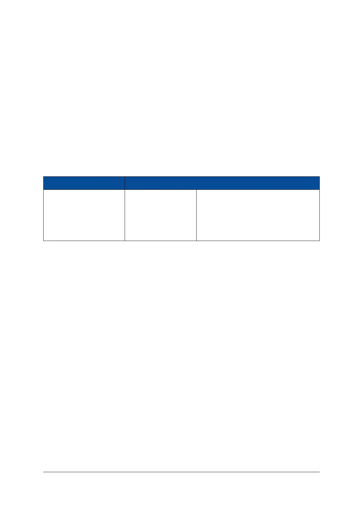
I/O Name Module Connector Pin Description
IO_B64_AF17_LS A-88
These pins have a level shifter from VCC_1V2
IO_B64_AC19_LS A-90
to VCC_CFG_MIO
IO_B64_AH16_LS A-92
IO_B64_AG19_LS A-94
Table 7: I/O Pin Exceptions - Level Shifters
The level shifters used for the I/O pins mentioned in Table 7 are NXP NTB0104 and the maximum achievable
data rate on these pins is 30 Mbit/sec.
2.9.3 Differential I/Os
When using differential pairs, a differential impedance of 100 Ω must be matched on the base board, and
the two nets of a differential pair must have the same length.
The information regarding the length of the signal lines from the MPSoC device to the module connector is
available in Mercury+ XU8 SoC Module IO Net Length Excel Sheet [3]. This enables the user to match the
total length of the differential pairs on the base board if required by the application.
The I/Os in the HD banks (N, O) can be used only as differential inputs when LVDS/LVPECL standards are
used; LVDS/LVPECL outputs are not supported.
Internal differential termination is not supported for the HD pins; all differential signal pairs from both HD
banks may optionally be equipped with 100 Ω differential termination resistors on the module. Refer to
Section 2.9.6 for details.
2.9.4 I/O Banks
Table 8 describes the main attributes of the Programmable Logic (PL) and Processing System (PS) I/O banks,
and indicates which peripherals are connected to each I/O bank. All I/O pins within a particular I/O bank
must use the same I/O (VCC_IO) and reference (VREF) voltages.
D-0000-454-001 19 / 60 Version 06, 18.11.2019
 Loading...


