Do you have a question about the Enclustra Mercury+ XU8 and is the answer not in the manual?
Covers general aspects, including introduction, warranty, and compliance.
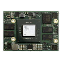
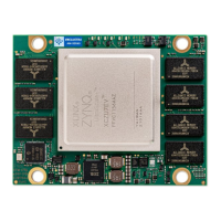
Introduces the Mercury+ XU8 SoC module, its components, and system capabilities.
Refers to general business conditions for warranty information.
Mentions compliance with the Restriction of Hazardous Substances Directive.
Addresses proper disposal and the inapplicability of the WEEE directive.
Provides critical safety advice for handling and using the module.
Lists the key features, specifications, and capabilities of the Mercury+ XU8 SoC module.
Details the items included with the Mercury+ XU8 SoC module package.
Describes optional accessories and related development tools for the module.
Explains the provided reference design for the Zynq UltraScale+ MPSoC.
Details the build system for Linux development on Enclustra SoC modules.
Lists the features and specifications of the Mercury+ PE1 base board.
Mentions supported Xilinx software tools for development with the module.
Illustrates the hardware architecture and component connections of the module.
Explains how module configurations and product codes are defined and interpreted.
Details the correspondence between module article numbers and article codes.
Shows visual representations of the module's physical top and bottom sides.
Displays the components and layout as seen from the top of the module.
Displays the components and layout as seen from the bottom of the module.
Provides assembly drawings for the module's top and bottom sides.
Shows the component placement and assembly for the top of the module.
Shows the component placement and assembly for the bottom of the module.
Details the physical footprint and mounting hole dimensions for base board integration.
Lists the mechanical specifications, dimensions, and weight of the module.
Describes the connectors used for interfacing with the base board.
Details the user-configurable Input/Output pins and their functionalities.
Provides information on the module's pinout and I/O bank assignments.
Lists specific I/O pins with special functions or restrictions.
Explains the usage and considerations for differential I/O pairs.
Describes the attributes and connectivity of the module's I/O banks.
Details how to manage VCC_IO voltages for compatibility and correct operation.
Covers signal termination strategies for differential and single-ended outputs.
Lists MIO pin connections and their suggested functions.
Explains the analog input capabilities and system monitor usage.
Describes the high-speed Multi-Gigabit Transceivers (GTH and GTR).
Details the GTH transceivers, their FPGA banks, and connections.
Details the GTR transceivers and their connections to the PS.
Covers the power supply, generation, and management aspects of the module.
Provides an overview of the on-board power supply generation from input voltage.
Explains the power control (PWR_EN) and status (PWR_GOOD) signals.
Lists the external voltage supply inputs required for the module operation.
Details the voltage supply outputs provided by the module to the base board.
Discusses factors affecting power consumption and estimation methods.
Addresses the need for cooling and lists compatible heat sinks.
Describes the voltage monitoring pins (VMON) for checking internal voltages.
Details the clock sources, frequencies, and connections for the module.
Explains the power-on reset (POR) and system reset (SRST) signals.
Describes the user LEDs and status LEDs located on the module.
Covers the DDR4 SDRAM connected to the Processing System (PS).
Lists the available DDR4 SDRAM types, densities, and configurations.
Refers to detailed information on DDR4 SDRAM connections.
Discusses signal termination requirements for DDR4 SDRAM.
Provides DDR4 SDRAM parameters for Vivado project setup.
Covers the DDR4 SDRAM connected to the Programmable Logic (PL).
Lists the available DDR4 SDRAM types for the PL.
Refers to detailed information on DDR4 SDRAM connections.
Discusses signal termination requirements for DDR4 SDRAM.
Provides DDR4 SDRAM parameters for Vivado project setup.
Describes the Quad SPI Flash memory for boot and storage.
Lists the available QSPI Flash types, sizes, and manufacturers.
Details the signals connected to the QSPI flash memory.
Explains the configuration options and speed for QSPI flash.
Discusses potential risks of QSPI flash corruption and mitigation.
Describes the eMMC Flash memory for boot and storage.
Lists the available eMMC Flash types, sizes, and manufacturers.
Details the signals connected to the eMMC flash memory.
Explains the interface and requirements for connecting an SD card.
Covers the dual Gigabit Ethernet interfaces and their configurations.
Lists the available Ethernet PHY types and manufacturers.
Details the Ethernet signal descriptions and dependencies.
Explains external connectivity options for the Ethernet interfaces.
Describes the MDIO interface and the addresses assigned to the PHYs.
Outlines the PHY configuration and bootstrap options.
Details RGMII delay configurations for optimal data sampling.
Covers the USB 2.0 interfaces and their configurations.
Lists the available USB 2.0 PHY types and manufacturers.
Details the USB 2.0 signal descriptions and dependencies.
Describes the built-in USB 3.0 controllers and PHYs.
Explains the built-in DisplayPort controllers and PHYs.
Details the on-module Real-Time Clock functionality and its connections.
Describes the secure EEPROM for storing module information.
Lists the available EEPROM types and manufacturers.
Details the signals used for MPSoC configuration and boot selection.
Explains the detection mechanism for Module Connector C.
Describes pull-up resistor configurations during device configuration.
Details the override for the PL power-on reset delay.
Explains the different boot modes available for the module.
Covers the Joint Test Action Group (JTAG) interface for debugging and configuration.
Explains JTAG connectivity on the module connector for PS and PL.
Describes external JTAG connections and recommendations.
Details how to boot the module using the JTAG interface.
Explains the process of booting the module from the eMMC flash.
Explains the process of booting the module from the QSPI flash.
Explains the process of booting the module from an SD card.
Describes methods for programming the eMMC flash memory.
Explains QSPI flash programming using the JTAG interface.
Details QSPI flash programming using an external SPI master.
Describes the Enclustra Module Configuration Tool for flash programming.
Provides an overview of the I2C bus, its connections, and speed limitations.
Details the signals used for I2C communication, including pull-ups.
Lists the addresses of devices connected on the I2C bus.
Explains the usage, content, and warnings for the secure EEPROM.
Details the memory map of the secure EEPROM's sectors.
Lists the absolute maximum ratings for various voltages and temperatures.
Provides the recommended operating conditions for reliable module performance.
Instructions for ordering the module or requesting information.
Information on accessing the Enclustra online support site.
| FPGA | Xilinx Zynq UltraScale+ |
|---|---|
| Processor Cores | Quad-core ARM Cortex-A53 |
| GPU | ARM Mali-400 MP2 |
| eMMC Capacity | 16 GB |
| Connectivity | Gigabit Ethernet, USB 3.0, USB 2.0 |
| PCIe | Gen2 x4 |
| Operating Temperature | -40 to +85 °C |
| Operating Temperature (Specific) | -40°C to +85°C (Industrial) |
| Dimensions | 100 mm x 100 mm |