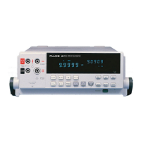
Option -05 IEEE-488 Interface
Introduction
8
8-3
8-1. Introduction
The IEEE-488 Interface turns the Fluke 45 into a fully programmable instrument for use
with the IEEE Standard 488.1 (1987) interface bus (IEEE-488 bus). With the IEEE-488
Interface, the Fluke 45 can become part of an automated instrumentation system.
8-2. Theory of Operation
8-3. Functional Block Description
The IEEE-488 Assembly (A5) requires power supply voltages, address, data and control
signals from the Fluke 45 Main Assembly (A1) to operate. The A5 assembly implements
the circuitry necessary to satisfy the IEEE-488.1 standard for programmable
instrumentation.
8-4. Detailed Circuit Description
The IEEE-488 Assembly comprises the following functional blocks: the Main Assembly
Connectors, the Address Decoding Circuit, the Isolation Circuits, the IEEE-488
Controller, and the IEEE-488 Transceivers and Connector. These five blocks are
described in the following paragraphs. Signal names mentioned during this discussion
are:
ACON*AC line power on
IRQ2*IEEE-488 interrupt request
OPSIEEE-488 option sense
OPTSW* IEEE-488 option power switch control signal
8-5. Main Assembly Connectors
The IEEE-488 Assembly interfaces with the Main Assembly through two ribbon cables
that mount to the 14-position and 20-position connectors on each assembly. The 20-pin
connector (A5J2) routes the 16-bit address bus from the Microprocessor (A1U6) to the
circuitry on the IEEE-488 Assembly. The 14-position connector (A5J3) passes the eight-
bit data bus and memory control signals between the two assemblies.
The IEEE-488 Assembly is powered by the +5.2V dc power supply (VCC) from the
Main Assembly. VCC is connected to the IEEE-488 Assembly via A5J3-1. The logic
common return (GND) is through A5J2-20.
8-6. Address Decoding Circuit
When a memory read or memory write cycle intended for the IEEE-488 Controller
(A5U6) is in progress, the 13 address bits ADD(15) through ADD(3) from A1U6 are
decoded by A5U1, A5U2, and A5U5 to generate an active low chip-select signal. The
chip-select signal (A5U5-8) goes low when two events occur: OPTSW* (A5J3-12) is
near -5.2V dc (VEE), and the address bus indicates that the Microprocessor is accessing
memory between addresses 0028 and 002F hexadecimal (inclusive). When the Fluke 45
is operating on battery power, the Microprocessor turns off the power to the IEEE-488
Assembly by driving the OPTSW* signal (A5J3-12) to VCC. This signal drives A5U1-6
to about +4.3V dc (through A5CR1), disabling the Address Decoding Circuit.

 Loading...