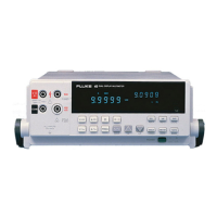
Option -05 IEEE-488 Interface
Theory of Operation
8
8-5
When the Microprocessor drives OPTSW* to VEE to enable the VCC2 power supply,
the CLR* input to the D flip-flop (A5U9-13) goes high to enable the flip-flop. The Q
output (A5U9-9) remains low until the Microprocessor does an initial dummy memory
cycle to the IEEE-488 Controller (approximately 1 ms later.) The rising edge at the end
of the chip select signal (A5U9-11) clocks the flip-flop and causes the Q output to go
high. This action removes the hardware reset to the IEEE-488 Controller. This delay is
followed by another dummy read cycle and a series of six memory write cycles that
program the IEEE-488 Controller.
For each character that it receives or transmits, the IEEE-488 Controller generates an
interrupt to the Microprocessor. These interrupts are generated by driving the open-drain
interrupt output A5U6-10 low. This signal is buffered by a tri-state buffer whose output
at A5U4-3 drives the IRQ2* input to the Microprocessor low. When the Microprocessor
responds to the interrupt and takes the necessary actions by reading and writing registers
in the IEEE-488 Controller, both A5U6-10 and, subsequently, A5U4-3 go high again.
Resistor A5R3 provides a pull-up termination on open-drain interrupt output A5U6-10.
Tri-state buffer output A5U4-3 is pulled up by resistor A5R2 to terminate the IRQ2*
signal when the buffer is tri-stated off.
When the Microprocessor performs a memory cycle to the IEEE-488 Controller, the
lower three bits of the address bus that are buffered by A5U4 (ADD(2) through ADD(0))
select the register being accessed in A5U6. When a memory read cycle is performed,
chip-enable A5U6-3 goes low, and A5U6-5 (DBIN) goes high. These actions enable
A5U6, driving the contents of the selected register onto the data bus and through the data
bus transceiver to the Microprocessor. When a memory write cycle is performed, chip-
enable A5U6-3 goes low, and A5U6-4 (WE*) goes first low and then high to latch the
data being driven from the Microprocessor (through A5U3) into the IEEE-488
Controller.
The IEEE-488 Controller interfaces to the IEEE-488 Transceivers using an eight-bit data
bus, eight interface signals, and two transceiver control signals (A5U6-33 and A5U6-
24).
The controller-in-charge signal (A5U6-33), which should always be high, controls the
direction of the SRQ, ATN, IFC, and REN IEEE-488 transceivers in A5U8.
The talk enable output (A5U6-24) is either low when the IEEE-488 Controller is not
addressed to talk or high when the controller is addressed to talk. This signal determines
the direction of all IEEE-488 Transceivers except SRQ, ATN, IFC, and REN.
8-9. IEEE-488 Transceivers/Connector
The IEEE-488 Transceivers (A5U7 and A5U8) are octal transceivers that are specifically
designed to exhibit the proper electrical drive characteristics to meet the IEEE-488
standard. These transceivers are configured to match the control signals available on the
IEEE-488 Controller. Assuming that A5U6-33 is always high, Table 8-1 describes the
transceiver direction control. The IEEE-488 Transceivers connect to a 24-position
connector, which mates with the ribbon cable leading to the IEEE-488 connector
mounted at the rear of the meter chassis.