Chapter 3 System configuration and assembly
21
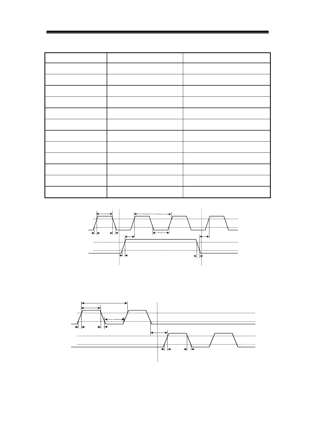
Table 3-5 Pulse input sequence parameter
Parameter Differential drive input Single terminal drive input
t
ck
>2µS >5µS
t
h
>1µS >2.5µS
t
l
>1µS >2.5µS
t
rh
<0.2µS <0.3µS
t
rl
<0.2µS <0.3µS
t
s
>1µS >2.5µS
t
qck
>8µS >10µS
t
qh
>4µS >5µS
t
ql
>4µS >5µS
t
qrh
<0.2µS <0.3µS
t
qrl
<0.2µS <0.3µS
t
qs
>1µS >2.5µS
t
h
t
l
t
rh
t
rl
t
s
t
s
t
ck
t
rh
t
rl
90%
90%
10%
10%
CW
CW
CCW
PULS
SIGN
Fig. 3.9 Sketch map of pulse +sign input interface time sequence
(max. pulse frequency 500kHz)
t
h
t
l
t
rh
t
rl
t
s
t
ck
t
rh
t
rl
10%
10%
90%
90%
CCW
CW
PULS
SIGN
Fig. 3.10 CCW pulse /CW pulse input interface time sequence (max.
pulse frequency 500kHz)