The post regulating circuitry contains regulators for
+
12V, -12V and
+5
V
(shown
as
+5V(F1)). There is additional circuitry to derive a
filtered
+
5
V
from the power supply
+
5
V
for the digital circuitry.
The
+
12
and +5
V
regulators are driven by the
+
15
V
supply from
the
A2
assembly. The -12
V
regulator
is
driven by the -15
V
supply
from the
A2
assembly. There are indication LEDs on the motherboard
for the five power supplies
that
are
lit
when the power supplies are
on.
The diagnostic latches latch signals from around the instrument that
are read by the controller during power-up.
A4
Reference
The reference assembly accepts either an external 10
MHz
reference
signal to lock the internal 10
MHz
TCXO
(temperature-compensated
crystal oscillator) or uses an optional high stability 10
MHz
OCXO
(oven-controlled crystal oscillator). The reference assembly outputs
two 200 kHz signals, a 1
GHz
signal, and
a
10
MHz
signal which is
routed to the rear panel.
One of the two 200
kHz
signals
is
routed to the
A5
synthesizer and
the other to the A3 modulation section. The 1
GHz
signal is routed to
the
A6
output assembly.
The 10
MHz
REF OUTPUT rear-panel signal is a buffered output from
the 10
MHz
TCXO
or
OCXO.
The 200
kHz
signals are derived by dividing the
10
MHz
signal by
50.
The 1
GHz
signal is derived from a 1
GHZ
VCO
that is phase-locked to
the 10
MHz
signal.
The reference assembly contains a calibration
ROM
that contains
factory-generated calibration data that is specific to the assembly.
A5
Sig
Gen Synth
The synthesizer assembly uses a 200
kHz
reference signal from the A4
reference assembly and generates a
500
to 1000
MHz
signal using a
divide-by-n phase-locked loop
VCO.
Frequency and phase modulation
are also done in the synthesizer assembly. The frequency is modulated
both inside and outside of the loop bandwidth. FM outside
of
the
loop bandwidth is summed with the integrator error voltage and
applied directly to the
VCO.
FM within the loop bandwidth and phase
modulation signals are applied to a phase modulator along with the
signal from the divide-by-n circuitry and then applied
to
the phase
detector.
The synthesizer assembly contains a calibration
ROM
that contains
factory-generated calibration data that is specific
to
the assembly.
A6
Output
The output assembly takes the
500
to 1000
MHz
signal from the A5
assembly and the
1
GHz
LO
signal from the A4 assembly to generate
the output frequency range of 0.25 to
1000
MHz
in three bands. The
output assembly also handles the filtering,
AM,
and amplitude leveling
functions.
The three frequency bands range from 0.25 to 249
MHz,
249 to
501
MHz,
and 501 to 1000
MHz.
The 0.25 to 250
MHz
band is heterodyned
from the
1
GHz
LO
signal and the
500
to 1000
MHz
main band signal.
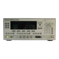
5a.4
Theory
of
Operation