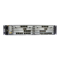
Figure 5-14 shows the functional block diagram of the AND3ML1A/AND3ML1B.
Figure 5-14 Functional block diagram of the AND3ML1A/AND3ML1B
Clock
module
Power
supply
module
Service access
module
Management
module
16 x E1 Service signal
Service
processing
module
Service signal
Backplane
3.3V
1V
.
.
.
.
.
.
-48V/-60V
-48V/-60V
Line clocks
Line clocks
System clocks
Management bus
Management bus
CXP
CXP
CXP
CXP
System
power supply
System
power supply
Transmit Direction
The service signals from the AND1CXPA/AND1CXPB are sent to the service processing
module. The service processing module performs PWE3 decapsulation and PW scheduling for
the service signals, processes the service signals based on the IMA/ATM, CES, and ML-PPP
protocols, performs the E1 framing function, and sends the service signals to the service access
module. The service access module performs encoding and line drive for the signals and outputs
the signals through the backplane-side interfaces.
Receive Direction
The board accesses service signals through the backplane-side interfaces, and then the signals
are sent to the service access module. The service access module performs interference isolation,
lightning-proof, impedance matching, level conversion, signal balancing, decoding, and then
sends the processed signals to the service processing module. The service processing module
performs E1 framing, processes service signals based on the IMA/ATM, CES, and ML-PPP
protocols, implements PWE3 encapsulation and PW scheduling, and sends the signals to the
AND1CXPA/AND1CXPB through the backplane-side interfaces.
Service Access Module
This module performs the following functions:
l In the receive direction, this module isolates common mode interference, protects circuits
against transient failures, matches the impedance in the receive direction with the internal
impedance, and performs level conversion, balancing, and decoding for the service signals.
Finally, this module sends the processed signals to the service processing module.
l In the transmit direction, this module receives the service signals from the service
processing module, encodes the signals, drives the line, and outputs the service signals
through the backplane-side interfaces.
ATN 950B Multi-service Access Equipment
Hardware Description 5 Physical Interface Card
Issue 03 (2012-07-23) Huawei Proprietary and Confidential
Copyright © Huawei Technologies Co., Ltd.
70
 Loading...