Trigger circuits
Buffering for Trigger Link input and output is performed by U146. Trigger input and output
is controlled by the IRQ4 and PB3 lines of the MPU. U164 provides additional logic for the
trigger input to minimize MPU control overhead.
At the factory, trigger output is connected to line 1 of the Trigger Link connector (resistor
R267 installed). Trigger input is connected to line 2 of the Trigger Link connector (resistor R270
installed).
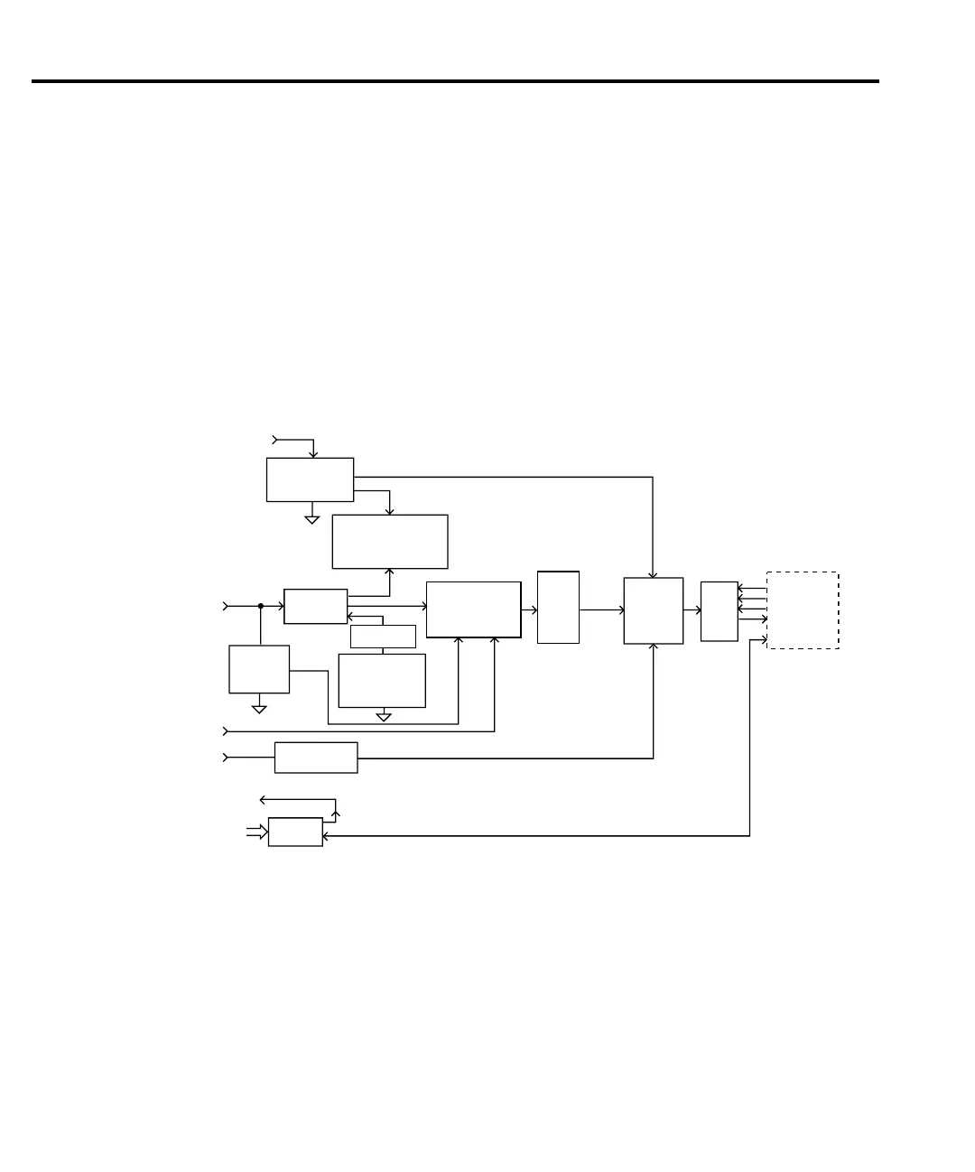
Analog circuitry
Refer to Figure 4-3 for the following discussion on analog circuitry.
INPUT HI
INPUT HI protection is provided by the SSP (solid state protection) circuit. The SSP is
primarily made up of Q101 and Q102. An overload condition opens Q101 and Q102, which
disconnects the analog input signal from the rest of the analog circuit.
Note that for the 100VDC and 1000VDC ranges, Q101 and Q102 of the SSP are open. The
DC voltage signal is routed through the DCV Divider (Q114 and Q136) to the DCV switching
circuit.
AMPS
Current Shunts
Q165, Q164, K103,
R158, R205, R386,
R450
DCA
ACA
AC Switching
&
Gain
K102, U102, U103, U105,
U112, U118, U111, U110
ACV,
FREQ
INPUT
HI
SSP*
Q101, Q102
DCV
OHMS
DCV
Divider
R117, Q109,
Q114, Q136
Ohms I-Source
U133, Q123, Q125,
Q124, Q126, Q119,
Q166, U123
DCV/100
DCV & Ohms
Switching
Q104, Q105,
Q108, Q113
SENSE
HI
X1
Buffer
Q137,
Q138,
U166,
U167
BUFCOM
A/D
MUX &
Gain
U163, U177,
U176, Q156
ADC
U165
Digital
Circuitry
(See Figure 4-2)
SENSE
LO
Protection
R373, Q121, Q135
Scanner Output
Scanner
Inputs
Scanner
Option
Scanner Control
*Solid State Protection
K101
SSP
Q153, CR132
gure
-
nalog circuitry block
diagram
4-8 Troubleshooting