© Microhard Systems Inc. Confidential 27
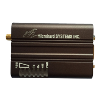
2.0 Hardware Description
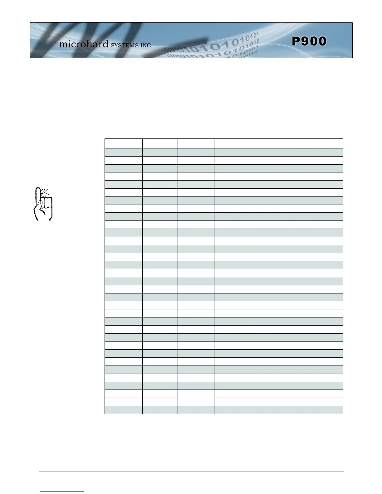
Pin Name P900 Pin No. n920 Pin No. Description
USR1 7 35
*Currently Not Supported. For Future Expansion*
USR2 8 37
*Reserved for future use.*
USR3 9 39
*Reserved for future use.*
USR_AN0 15 9
Analog Input 0. *Future Use.*
USBDP 18 25
*Currently Not Supported. For Future Expansion*
USBDM 19 21
*Currently Not Supported. For Future Expansion*
LED_1 (RSSI1) 20 30 Receive Signal Strength Indicator 1.
LED_2 (RSSI2) 21 28 Receive Signal Strength Indicator 2.
LED_3 (RSSI3)
22 26
Receive Signal Strength Indicator 3.
LED_RX 23 22 Active high output indicates receive and synchronization status.
LED_TX 24 24 Active high output indicates module is transmitting RF data.
Serial RING 27 38
*Reserved for future use.*
Serial RxD 28 42 Receive Data. Logic level input into the modem.
Serial TxD 29 44 Transmit Data. Logic level Output from the modem.
Serial DSR 30 36 Data Set Ready. Active low output.
Serial CTS 31 32 Clear To Send. Active low output.
Serial DTR 32 40 Data Terminal Ready. Active low input.
Serial DCD 33 46 Data Carrier Detect. Active low output.
Serial RTS 34 34 Request To Send. Active low input.
USR SCK 35 50
*Currently Not Supported. For Future Expansion*
Control RxD 37 20 Diagnostics receive data.
Control TxD 38 18 Diagnostics transmit data.
Vbat 42 17 Battery Voltage sensing analog input line.
RSMode 44 19
*Reserved for future use.*
!RESET 45 15 Active low input will reset the module.
!CONFIG 46 13 Active low input signal to put module into default serial mode.
Wakeup_usr 47 11 Active high input used to wake the model from sleep mode.
!Bootpgm_mode 48 7
*Reserved for future use.*
CANTX 50 12
*Currently Not Supported. For Future Expansion*
CANRX 51 10
*Currently Not Supported. For Future Expansion*
Vdd 62 Positive voltage supply voltage for the digital section of the module (3.3V).
51,53,55,57,59
Vcc 63,64 Positive voltage supply voltage for the radio module (3.3V).
Vcc2 75,76,77 N/A
*Reserved for future use.*
Table 2-15: P900 to Nano n920 Pin Description
For detailed pin
descriptions refer to
Section 2.3 Pin Description.
2.5 P900 to Nano n920 Pin-Outs
The following table shows a pin-out comparison between the P900 and the n920. This table
may be useful for customers who current have the n920 who wish to migrate to the P900
platform.