Theory of Operation: Controller 3-33
3.2.4.6 Synchronous External Memory Interface
This interfaces the OMAP to a 32 MB Double Data Rate (DDR) RAM IC (U6301). Upon boot-up
OMAP configures this interface to operate in synchronous mode at 96MHz. This volatile memory unit
is primarily accessed during code execution.
3.2.4.7 Double Data Rate (DDR) Memory (U6301)
The 32MB DDR Synchronous DRAM IC is interfaced to the OMAP using 13 address bits and a 16bit
data bus. The DDR IC is driven by a complementary clock signal originating from the OMAP IC. The
DDR clock is initialized to 96MHz by the OMAP boot code. Additional control signals are also
dedicated for the DRAM interface
.
3.2.4.8 Peripheral Devices
The OMAP processor is equipped with multiple buses and interfaces that are configured for
peripheral interconnection.
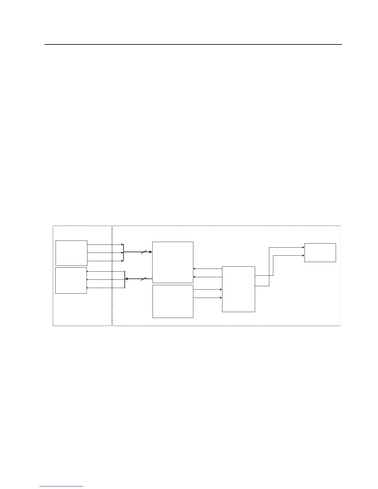
3.2.4.8.1 Receive and Transmit SSI
These two interfaces are dedicated for communicating with the RF deck digital interface, carrying
receive and transmit base band signals. The OMAP processor generates the clock and FSYNC
signals for the receive SSI interface. The RF deck generates these signals for the transmit SSI
interface.
Figure 3-22. RX / TX SSI Configuration
RF SECTION
TRIDENT
ABACUS
RX_FSYNC
RX_CLK
RX_DA
TX_FSYNC
TX_CLK
TX_DA
CONTROLLER SECTION
OMAP 1710
MAKO
TI
CODEC
McBSP 2
McBSP 1
RX SSI
TX SSI
3
3
VC_FSYNC
VC_DCLK
SYNC
BCLK
McBSP 2
CPLD
MCLK
WCLK
 Loading...