41
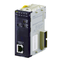
Transistor Remote I/O Terminals Section 4-3
Setting Pins 9 and 10 The functions of pins 9 and 10 differ for inputs and outputs, as shown in the
following diagram.
Pin 9: Reserved (Always OFF)
Pin 10: As follows:
Inputs: No function (Always OFF)
Outputs: Hold/Clear outputs for communications error
OFF (Clear): All output data from the Master will be cleared to 0 when a
communications error occurs.
ON (Hold): All output data from the Master will be retained when a
communications error occurs.
Pins 9 and 10 are factory-set to OFF.
4-3-2 Transistor Remote Input Terminals with 8 Points:
DRT1-ID08 (NPN) and DRT1-ID08-1 (PNP)
Input Specifications
Input: Not used (Always OFF)
Output: Hold/Clear outputs for communications error
Reserved: Always OFF
Item Specification
Model DRT1-ID08 DRT1-ID08-1
Internal I/O common NPN PNP
Input points 8 points (allocated one word in Master)
ON voltage 15 V DC min. (between
each input terminal and V)
15 V DC min. (between
each input terminal and G)
OFF voltage 5 V DC max. (between
each input terminal and V)
5 V DC max. (between
each input terminal and G)
OFF current 1 mA max.
Input current 10 mA max./point
ON delay time 1.5 ms max.
OFF delay time 1.5 ms max.
Number of circuits 8 points with one common

 Loading...