R8C/1A Group, R8C/1B Group 14. Timers
Rev.1.30 Dec 08, 2006 Page 131 of 315
REJ09B0252-0130
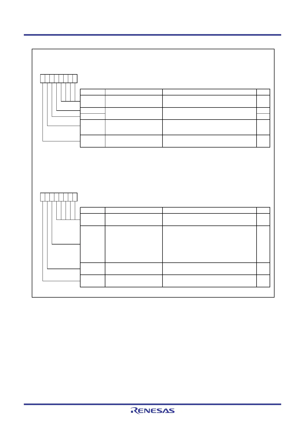
Figure 14.17 Registers TZMR and PUM in Programmable Waveform Generation Mode
Timer Z Waveform Output Control Register
Symbol Address After Reset
PUM
0084h 00h
Bit Symbol Bit Name Function RW
INT0
____
pin one-shot trigger
control bit
INT0
____
pin one-shot trigger
polarity select bit
0
b3 b2
INOSTG
b1 b0
0
—
(b4-b0)
000 0
b7 b6 b5 b4
RW
TZOPL RW
0
Reserved bits Set to 0.
Timer Z output level latch 0 : Outputs “H” for primary period.
Outputs “L” for secondary period.
Outputs “L” w hen the timer is stopped.
1 : Outputs “L” for primary period.
Outputs “H” for secondary period.
Outputs “H” w hen the timer is stopped.
RW
INOSEG RW
Set to 0 in programmable w aveform generation
mode.
Set to 0 in programmable w aveform generation
mode.
Timer Z Mode Register
Symbol Address After Reset
TZMR
0080h 00h
Bit Symbol Bit Name Function RW
NOTES :
1.
2.
When the TZS bit is set to 1 (count starts), the count value is w ritten to the reload register only. When the TZS bit is
set to 0 (count stops), the count value is w ritten to both reload register and counter.
TZS
Timer Z count start flag
(2)
0 : Stops counting.
1 : Starts counting.
RW
TZWC
Timer Z w rite control bit Set to 1 in programmable w aveform generation
mode.
(1)
RW
Reserved bits Set to 0.
RW
TZMOD0 Timer Z operating mode bits
b5 b4
0 1 : Programmable w aveform generation mode
RW
TZMOD1 RW
000
—
(b3-b0)
1010
Refer to
14.2.5 Notes on Timer Z
for precautions regarding the TZS bit.
b7 b6 b5 b4 b3 b2 b1 b0
 Loading...


