R8C/1A Group, R8C/1B Group 16. Clock Synchronous Serial Interface
Rev.1.30 Dec 08, 2006 Page 222 of 315
REJ09B0252-0130
16.3.4 Clock Synchronous Serial Mode
16.3.4.1 Clock Synchronous Serial Format
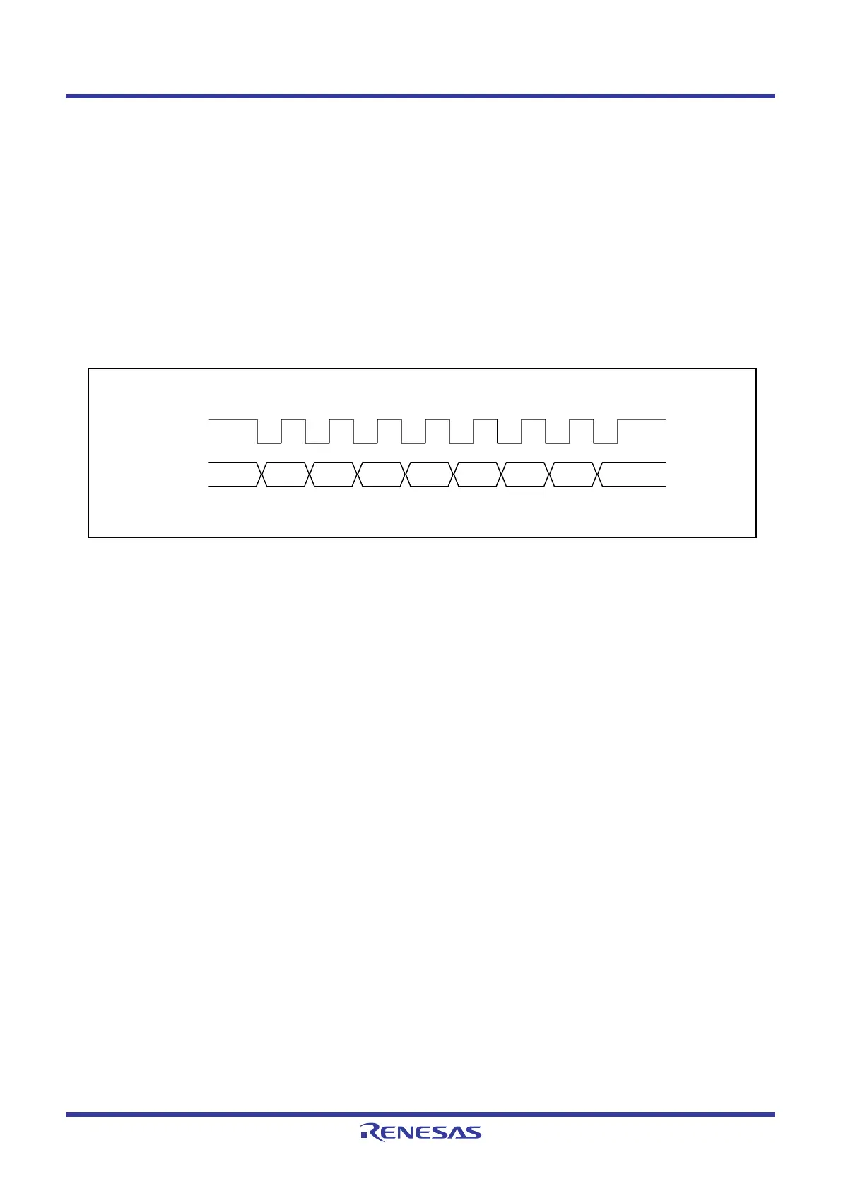
Set the FS bit in the SAR register to 1 to use the clock synchronous serial format for communication.
Figure 16.41 shows the Transfer Format of Clock Synchronous Serial Format.
When the MST bit in the ICCR1 register is set to 1, the transfer clock is output from the SCL pin, and when the
MST bit is set to 0, the external clock is input.
The transfer data is output between successive falling edges of the SCL clock, and data is determined at the
rising edge of the SCL clock. MSB-first or LSB-first can be selected as the order of the data transfer by setting
the MLS bit in the ICMR register. The SDA output level can be changed by the SDAO bit in the ICCR2 register
during transfer standby.
Figure 16.41 Transfer Format of Clock Synchronous Serial Format
SCL
b0
SDA b1 b2 b3 b4 b5 b6 b7
 Loading...


