R8C/1A Group, R8C/1B Group 1. Overview
Rev.1.30 Dec 08, 2006 Page 12 of 315
REJ09B0252-0130
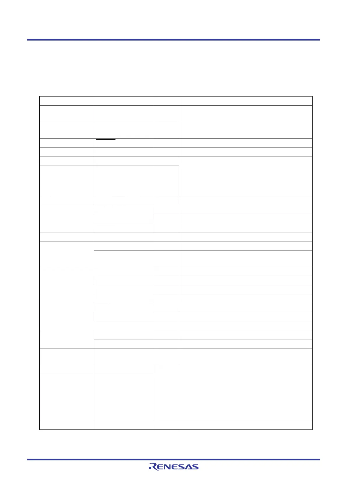
1.6 Pin Functions
Table 1.5 lists Pin Functions, Table 1.6 lists Pin Name Information by Pin Number of PLSP0020JB-A,
PRDP0020BA-A Packages and Table 1.7 lists Pin Name Information by Pin Number of PWQN0028KA-
B Package.
I: Input O: Output I/O: Input and output
Table 1.5 Pin Functions
Type Symbol I/O Type Description
Power Supply Input VCC, VSS I Apply 2.7 V to 5.5 V to the VCC pin.
Apply 0 V to the VSS pin.
Analog Power
Supply Input
AVCC, AVSS I Power supply for the A/D converter
Connect a capacitor between AVCC and AVSS.
Reset Input RESET
I Input “L” on this pin resets the MCU.
MODE MODE I Connect this pin to VCC via a resistor.
Main Clock Input XIN I These pins are provided for main clock generation
circuit I/O. Connect a ceramic resonator or a
crystal oscillator between the XIN and XOUT pins.
To use an external clock, input it to the XIN pin
and leave the XOUT pin open.
Main Clock Output XOUT O
INT
Interrupt INT0, INT1, INT3 I INT interrupt input pins
Key Input Interrupt KI0
to KI3 I Key input interrupt input pins
Timer X CNTR0 I/O Timer X I/O pin
CNTR0
O Timer X output pin
Timer Z TZOUT O Timer Z output pin
Timer C TCIN I Timer C input pin
CMP0_0 to CMP0_2,
CMP1_0 to CMP1_2
O Timer C output pins
Serial Interface CLK0 I/O Transfer clock I/O pin
RXD0, RXD1 I Serial data input pins
TXD0, TXD1 O Serial data output pins
Clock synchronous
serial I/O with chip
select (SSU)
SSI00, SSI01 I/O Data I/O pin.
SCS
I/O Chip-select signal I/O pin
SSCK I/O Clock I/O pin
SSO I/O Data I/O pin
I
2
C bus Interface
SCL I/O Clock I/O pin
SDA I/O Data I/O pin
Reference Voltage
Input
VREF I Reference voltage input pin to A/D converter
A/D Converter AN8 to AN11 I Analog input pins to A/D converter
I/O Port P1_0 to P1_7,
P3_3 to P3_5, P3_7,
P4_5
I/O CMOS I/O ports. Each port has an I/O select
direction register, allowing each pin in the port to
be directed for input or output individually.
Any port set to input can be set to use a pull-up
resistor or not by a program.
P1_0 to P1_3 also function as LED drive ports.
Input Port P4_2, P4_6, P4_7 I Input-only ports
 Loading...


