R8C/1A Group, R8C/1B Group 16. Clock Synchronous Serial Interface
Rev.1.30 Dec 08, 2006 Page 183 of 315
REJ09B0252-0130
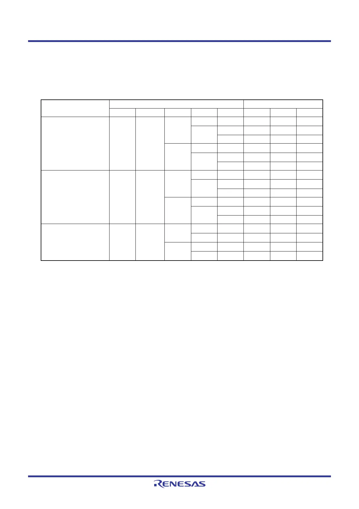
16.2.4 Communication Modes and Pin Functions
Clock synchronous serial I/O with chip select switches the functions of the I/O pins in each communication
mode according to the setting of the MSS bit in the SSCRH register and bits RE and TE in the SSER register.
Table 16.4 shows the Association between Communication Modes and I/O Pins.
NOTES:
1. This pin can be used as a programmable I/O port.
2. Do not set both bits TE and RE to 1 in 4-wire bus (bidirectional) communication mode.
SSUMS and BIDE: Bits in SSMR2 register
MSS: Bit in SSCRH register
TE and RE: Bits in SSER register
Table 16.4 Association between Communication Modes and I/O Pins
Communication Mode
Bit Setting Pin State
SSUMS BIDE MSS TE RE SSI SSO SSCK
Clock synchronous
communication mode
0Disabled001Input
−
(1)
Input
10
−
(1)
Output Input
1 Input Output Input
101Input
−
(1)
Output
10
−
(1)
Output Output
1 Input Output Output
4-wire bus
communication mode
10 001
−
(1)
Input Input
1 0 Output
−
(1)
Input
1 Output Input Input
101Input
−
(1)
Output
10
−
(1)
Output Output
1 Input Output Output
4-wire bus
(bidirectional)
communication mode
(2)
11 001
−
(1)
Input Input
10
−
(1)
Output Input
101
−
(1)
Input Output
10
−
(1)
Output Output
 Loading...


