R8C/1A Group, R8C/1B Group 16. Clock Synchronous Serial Interface
Rev.1.30 Dec 08, 2006 Page 211 of 315
REJ09B0252-0130
16.3.3 I
2
C bus Interface Mode
16.3.3.1 I
2
C bus Format
Setting the FS bit in the SAR register to 0 communicates in I
2
C bus format.
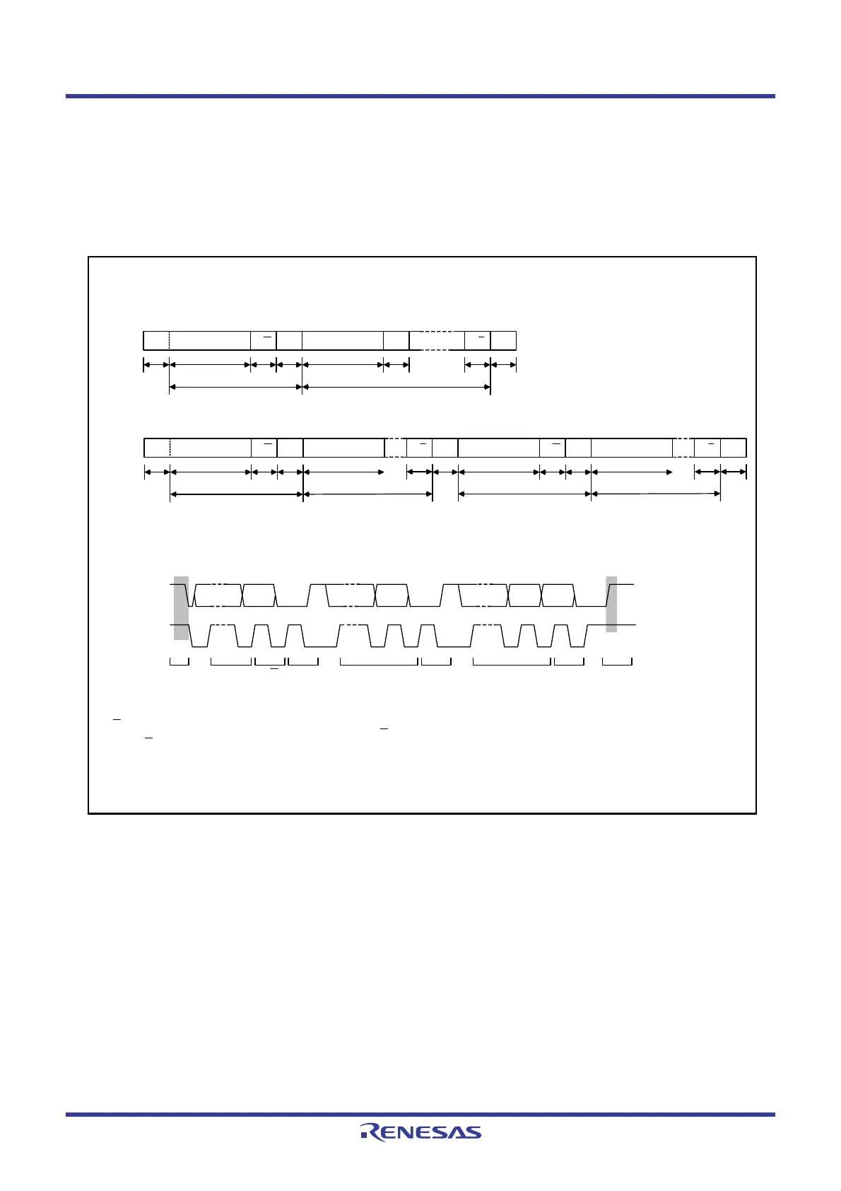
Figure 16.32 shows the I
2
C bus Format and Bus Timing. The 1st frame following the start condition consists of
8 bits.
Figure 16.32 I
2
C bus Format and Bus Timing
S R/W A DATA A A/A P
1
7
1 1
n
1 1 1
1 m
(a) I
2
C bus format (FS = 0)
Transfer bit count (n = 1 to 8)
Transfer frame count (m = from 1)
S R/W A
DATA
A/A P
1
7
1 1
n1
1 1
1 m1
(b) I
2
C bus format (when start condition is retransmitted, FS = 0)
Upper: Transfer bit count (n1, n2 = 1 to 8)
Lower: Transfer frame count (m1, m2 = 1 or more)
SLA
SLA
A/A
1
S
1
R/W A
DATA
7
1 1
n2
SLA
1 m2
SDA
SCL
S
SLA R/W A DATA A DATA A P
1 to 7 8 9 1 to 7 8 9 1 to 7 8 9
(1) I
2
C bus format
(2) I
2
C bus timing
Explanation of symbols
S : Start condition
The master device changes the SDA signal from “H” to “L” while the SCL signal is held “H”.
SLA : Slave address
R/W : Indicates the direction of data transmit/receive
Data is transmitted from the slave device to the master device when R/W value is 1 and from the master device to the slave device when
R/W value is 0.
A : Acknowledge
The receive device sets the SDA signal to “L”.
DATA : Transmit / receive data
P : Stop condition
The master device changes the SDA signal from “L” to “H” while the SCL signal is held “H”.
 Loading...


