R8C/1A Group, R8C/1B Group 14. Timers
Rev.1.30 Dec 08, 2006 Page 142 of 315
REJ09B0252-0130
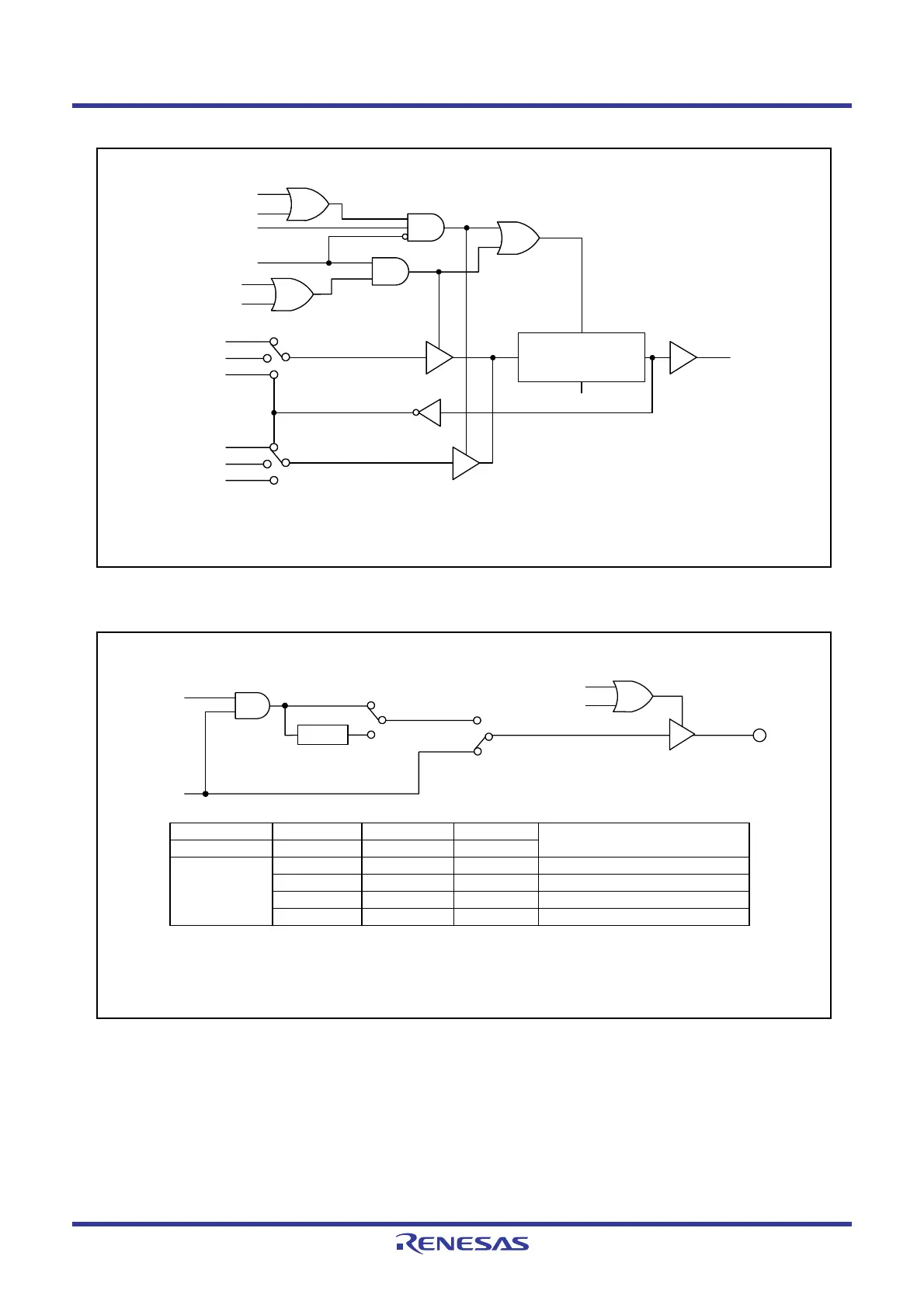
Figure 14.24 Block Diagram of CMP Waveform Generation Unit
Figure 14.25 Block Diagram of CMP Waveform Output Unit
TCC14
CMP output
(internal signal)
TCC14 to TCC17: Bits in TCC1 register
Latch
DQ
= 11b
= 10b
“L”
“H”
= 01b
Reverse
TCC17 to TCC16
= 01b
= 10b
“L”
“H”
= 11b
TCC15 to TCC14
T
TCC15
Compare 0 interrupt signal
TCC16
TCC17
R
Reset
Compare 1 interrupt signal
Reverse
Register TCOUT P1 TCOUT
Bit TCOUT0 P1_0 TCOUT6
Setting Value 1 1 0 CMP0_0 waveform output
1 1 1 CMP0_0 reversed waveform output
1 0 0 “L” output
1 0 1 “H” output
CMP0_0 Output
CMP output
(Internal signal)
Reverse
TCOUT6 = 0
PD1_0
TCOUT0
TCOUT6 = 1
TCOUT0 = 1
TCOUT0 = 0
CMP0_0
P1_0
This diagram is a block diagram of the CMP0_0 waveform output unit.
The CMP0_1 to CMP0_2 and CMP1_0 to CMP1_2 waveform output units have the same configuration.
 Loading...


