R8C/1A Group, R8C/1B Group 15. Serial Interface
Rev.1.30 Dec 08, 2006 Page 154 of 315
REJ09B0252-0130
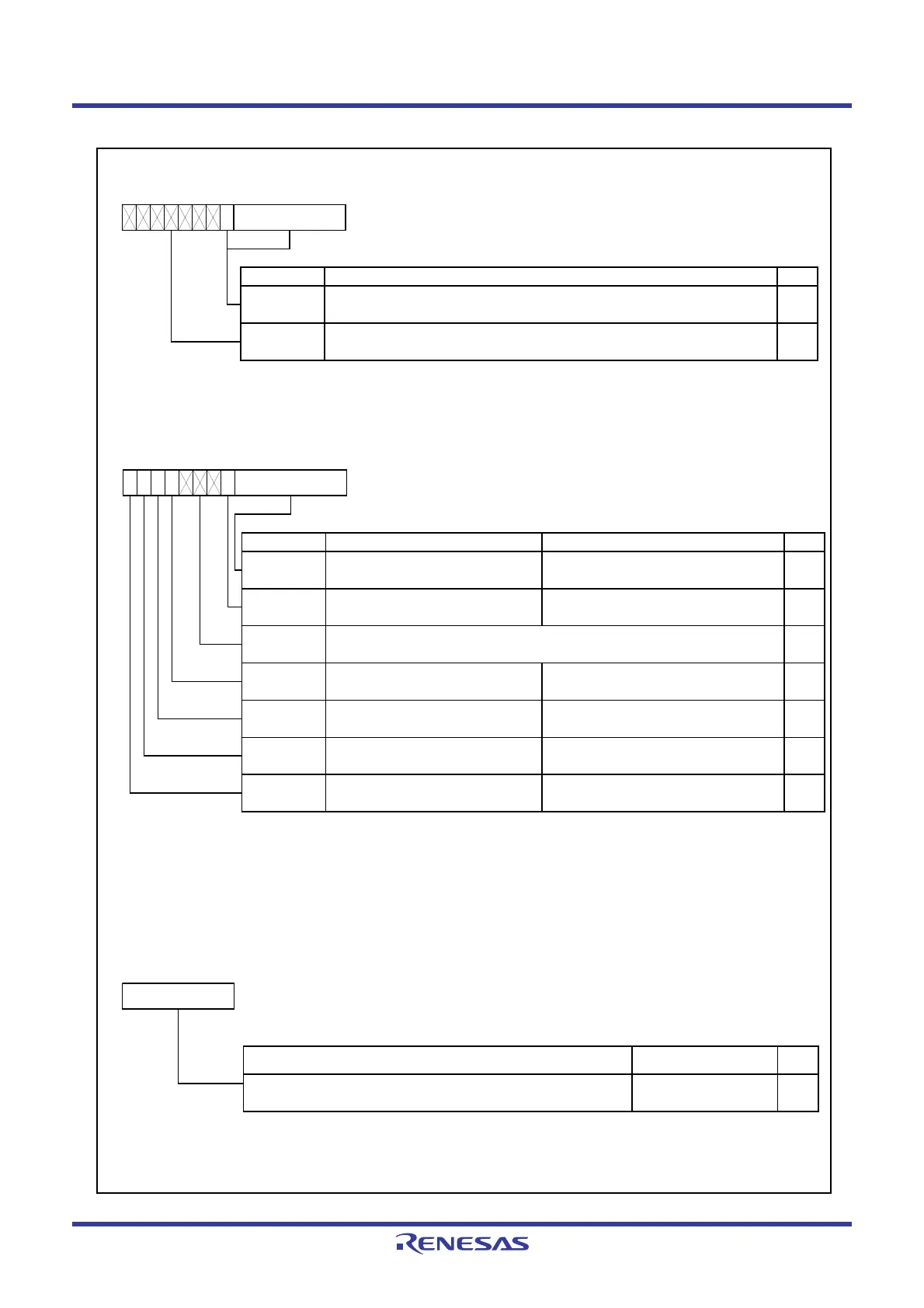
Figure 15.3 Registers U0TB to U1TB, U0RB to U1RB, and U0BRG to U1BRG
UARTi Transmit Buffer Register (i = 0 or 1)
(1, 2)
Symbol Address After Reset
U0TB
00A3h-00A2h Undefined
U1TB
00ABh-00AAh Undefined
RW
NOTES :
1.
2.
(b15)
b7
(b8)
b0
b0b7
When the transfer data length is 9 bits, w rite data to high byte first, then low byte.
Use the MOV instruction to w rite to this register.
WO
—
FunctionBit Symbol
—
(b8-b0)
—
(b15-b9)
Transmit data
Nothing is assigned. If necessary, set to 0.
When read, the content is undefined.
UARTi Receive Buffer Register (i = 0 or 1)
(1)
Symbol Address After Reset
U0RB
00A7h-00A6h Undefined
U1RB
00AFh-00AEh Undefined
RW
NOTES :
1.
2.
Read out the UiRB register in 16-bit units.
Bits SUM, PER, FER, and OER are set to 0 (no error) w hen bits SMD2 to SMD0 in the UiMR register are set to 000b
(serial interface disabled) or the RE bit in the UiC1 register is set to 0 (receive disabled). The SUM bit is set to 0 (no
error) w hen bits PER, FER, and OER are set to 0 (no error). Bits PER and FER are set to 0 even w hen the higher byte
of the UiRB register is read out.
Also, bits PER and FER are set to 0 w hen reading the high-order byte of the UiRB register.
ROSUM
Error sum flag
(2)
0 : No error
1 : Error
RO
FER
Framing error flag
(2)
0 : No framing error
1 : Framing error
RO
PER
Parity error flag
(2)
0 : No parity error
1 : Parity error
OER
Overrun error flag
(2)
0 : No overrun error
1 : Overrun error
RO
Bit Symbol Bit Name
(b8)
b0
(b15)
b7
b0b7
Function
Receive data (D7 to D0)
RO
Receive data (D8)
RO
Nothing is assigned. If necessary, set to 0.
When read, the content is undefined.
—
(b11-b9)
—
—
(b7-b0)
—
—
(b8)
—
UARTi Bit Rate Register (i = 0 or 1)
(1, 2, 3)
Symbol Address After Reset
U0BRG
00A1h Undefined
U1BRG
00A9h Undefined
Setting Range RW
NOTES :
1.
2.
3. After setting the CLK0 to CLK1 bits of the UiC0 register, w rite to the UiBRG register.
b7
Use the MOV instruction to w rite to this register.
WO
Write to this register w hile the serial I/O is neither transmitting nor receiving.
00h to FFh
Function
Assuming the set value is n, UiBRG divides the count source by n+1
b0
 Loading...


