R8C/1A Group, R8C/1B Group 15. Serial Interface
Rev.1.30 Dec 08, 2006 Page 159 of 315
REJ09B0252-0130
NOTE:
1. Set bits which are not in this table to 0 when writing to the above registers in clock synchronous
serial I/O mode.
Table 15.3 lists the I/O Pin Functions in Clock Synchronous Serial I/O Mode. The TXD0 pin outputs “H” level
between the operating mode selection of UART0 and transfer start. (If the NCH bit is set to 1 (N-channel open-
drain output), this pin is in a high-impedance state.)
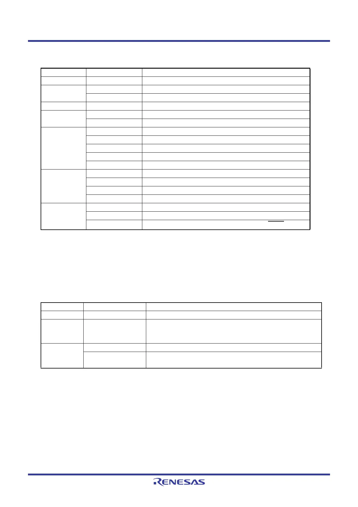
Table 15.2 Registers Used and Settings in Clock Synchronous Serial I/O Mode
(1)
Register Bit Function
U0TB 0 to 7 Set data transmission.
U0RB 0 to 7 Data reception can be read.
OER Overrun error flag
U0BRG 0 to 7 Set bit rate.
U0MR SMD2 to SMD0
Set to 001b.
CKDIR Select the internal clock or external clock.
U0C0 CLK1 to CLK0 Select the count source in the U0BRG register.
TXEPT Transmit register empty flag
NCH Select TXD0 pin output mode.
CKPOL Select the transfer clock polarity.
UFORM Select the LSB first or MSB first.
U0C1 TE Set this bit to 1 to enable transmission/reception.
TI Transmit buffer empty flag
RE Set this bit to 1 to enable reception.
RI Reception complete flag
UCON U0IRS Select the UART0 transmit interrupt source.
U0RRM Set this bit to 1 to use continuous receive mode.
CNTRSEL
Set this bit to 1 to select P1_5/RXD0/CNTR01/INT11
.
Table 15.3 I/O Pin Functions in Clock Synchronous Serial I/O Mode
Pin Name Function Selection Method
TXD0 (P1_4) Output serial data (Outputs dummy data when performing reception only.)
RXD0 (P1_5) Input serial data PD1_5 bit in PD1 register = 0
(P1_5 can be used as an input port when performing
transmission only.)
CLK0 (P1_6) Output transfer clock CKDIR bit in U0MR register = 0
Input transfer clock CKDIR bit in U0MR register = 1
PD1_6 bit in PD1 register = 0
 Loading...


