R8C/1A Group, R8C/1B Group 15. Serial Interface
Rev.1.30 Dec 08, 2006 Page 164 of 315
REJ09B0252-0130
NOTES:
1. The bits used for transmit/receive data are as follows: Bits 0 to 6 when transfer data is 7 bits long;
bits 0 to 7 when transfer data is 8 bits long; bits 0 to 8 when transfer data is 9 bits long.
2. An external clock can be selected in UART0 only.
Table 15.6 lists the I/O Pin Functions in Clock Asynchronous Serial I/O Mode. The TXDi pin outputs “H” level
between the operating mode selection of UARTi (i = 0 or 1) and transfer start. (If the NCH bit is set to 1 (N-channel
open-drain output), this pin is in a high-impedance state.)
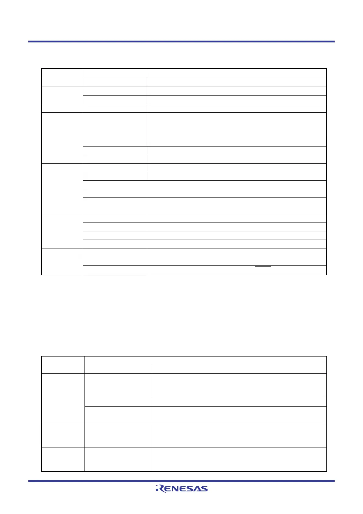
Table 15.5 Registers Used and Settings for UART Mode
Register Bit Function
UiTB 0 to 8
Set transmit data.
(1)
UiRB 0 to 8
Receive data can be read.
(1)
OER,FER,PER,SUM Error flag
UiBRG 0 to 7 Set a bit rate.
UiMR SMD2 to SMD0 Set to 100b when transfer data is 7 bits long.
Set to 101b when transfer data is 8 bits long.
Set to 110b when transfer data is 9 bits long.
CKDIR
Select the internal clock or external clock.
(2)
STPS Select the stop bit.
PRY, PRYE Select whether parity is included and whether odd or even.
UiC0 CLK0, CLK1 Select the count source for the UiBRG register.
TXEPT Transmit register empty flag
NCH Select TXDi pin output mode.
CKPOL Set to 0.
UFORM LSB first or MSB first can be selected when transfer data is 8 bits
long. Set to 0 when transfer data is 7 or 9 bits long.
UiC1 TE Set to 1 to enable transmit.
TI Transmit buffer empty flag
RE Set to 1 to enable receive.
RI Receive complete flag
UCON U0IRS, U1IRS Select the source of UART0 transmit interrupt.
U0RRM Set to 0.
CNTRSEL
Set to 1 to select P1_5/RXD0/CNTR01/INT11
.
Table 15.6 I/O Pin Functions in Clock Asynchronous Serial I/O Mode
Pin name Function Selection Method
TXD0(P1_4) Output serial data (Cannot be used as a port when performing reception only.)
RXD0(P1_5) Input serial data PD1_5 bit in PD1 register = 0
(P1_5 can be used as an input port when performing
transmission only.)
CLK0(P1_6) Programmable I/O Port CKDIR bit in U0MR register = 0
Input transfer clock CKDIR bit in U0MR register = 1
PD1_6 bit in PD1 register = 0
TXD1(P3_7) Output serial data Bits U1SEL1 to U1SEL0 in UCON register = 11b (P3_7 can be
used as a port when bits U1SEL1 to U1SEL0 = 01b and
performing reception only.)
RXD1(P4_5) Input serial data PD4_5 bit in PD4 register = 0
Bits U1SEL1 to U1SEL0 in UCON register = 01b or 11b
(Cannot be used as a port when performing transmission only.)
 Loading...


