R8C/1A Group, R8C/1B Group 16. Clock Synchronous Serial Interface
Rev.1.30 Dec 08, 2006 Page 180 of 315
REJ09B0252-0130
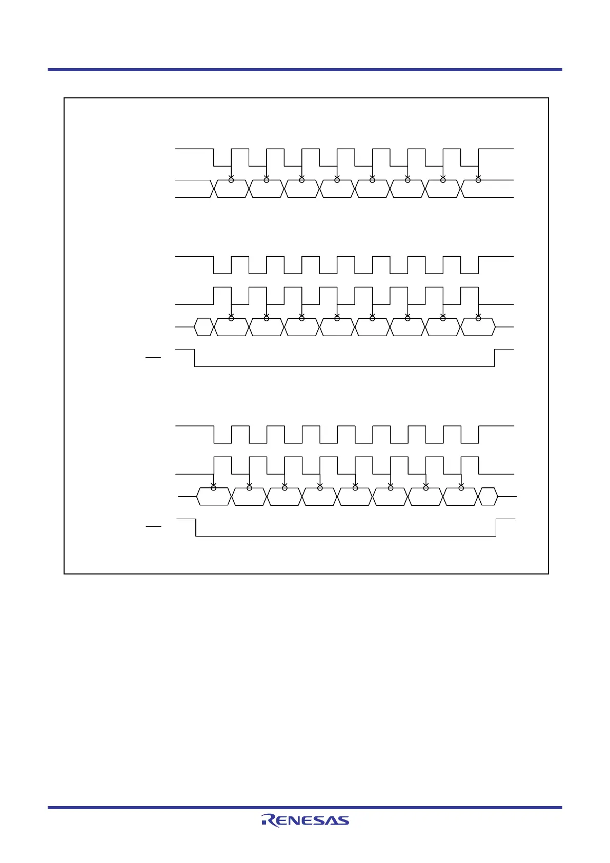
Figure 16.10 Association between Transfer Clock Polarity, Phase, and Transfer Data
SSCK
b0
SSO, SSI
• SSUMS = 0 (clock synchronous communication mode), CPHS bit = 0 (data change at odd
edge), and CPOS bit = 0 (“H” when clock stops)
b1 b2 b3 b4 b5 b6 b7
SSCK
CPOS = 0
(“H” when clock stops)
b0SSO, SSI
• SSUMS = 1 (4-wire bus communication mode) and CPHS = 0 (data change at odd edge)
b1 b2 b3 b4 b5 b6 b7
SSCK
CPOS = 1
(“L” when clock stops)
SCS
SSCK
CPOS = 0
(“H” when clock stops)
SSO, SSI
• SSUMS = 1 (4-wire bus communication mode) and CPHS = 1 (data download at odd edge)
SSCK
CPOS = 1
(“L” when clock stops)
SCS
b0 b1 b2
b3 b4
b5
b6
b7
CPHS and CPOS: Bits in SSMR register, SSUMS: Bits in SSMR2 register
 Loading...


