R8C/1A Group, R8C/1B Group 16. Clock Synchronous Serial Interface
Rev.1.30 Dec 08, 2006 Page 190 of 315
REJ09B0252-0130
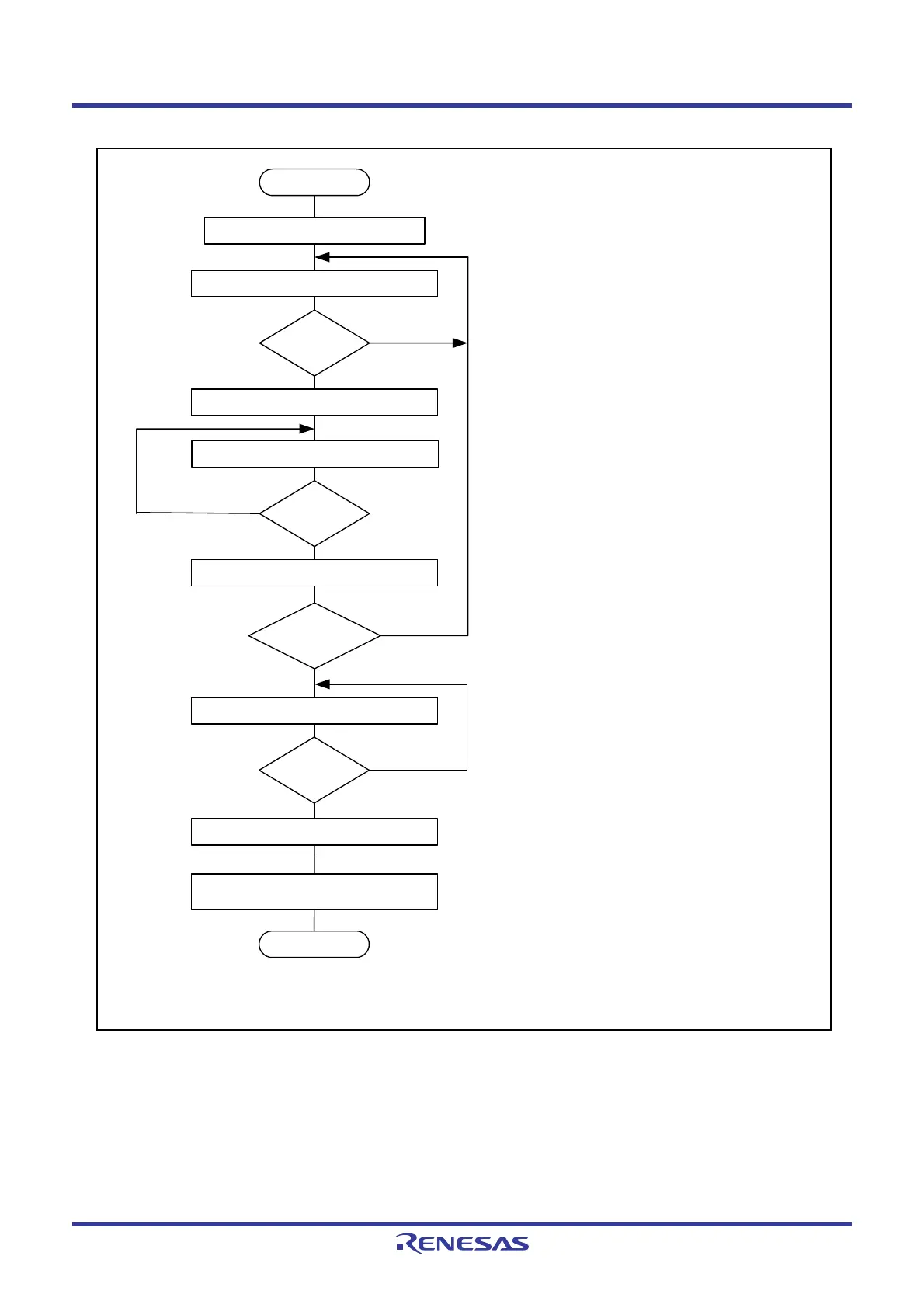
Figure 16.17 Sample Flowchart of Data Transmission/Reception (Clock Synchronous
Communication Mode)
Start
Initialization
Read TDRE bit in SSSR register
SSSR register TEND bit ← 0
(1)
End
TDRE = 1 ?
Write transmit data to SSTDR register
Data
transmission
continues?
No
Yes
Yes
No
SSER register RE bit ← 0
TE bit
← 0
(1)
(2)
(3)
(1) After reading the SSSR register and confirming
that the TDRE bit is set to 1, write the transmit
data to the SSTDR register. When the transmit
data is written to the SSTDR register, the TDRE
bit is automatically set to 0.
(5) Set the TEND bit to 0
(6) and bits RE and TE in the SSER register to 0 before
ending transmit/receive mode.
Read receive data in SSRDR register
Read RDRF bit in SSSR register
RDRF = 1 ?
No
Yes
(4)
(2) Confirm that the RDRF bit is set to 1. If the RDRF
bit is set to 1, read the receive data in the SSRDR
register. When the SSRDR register is read, the
RDRF bit is automatically set to 0.
(3) Determine whether data transmission continues.
(5)
NOTE:
1. Write 0 after reading 1 to set the TEND bit to 0.
Read TEND bit in SSSR register
TEND = 1 ?
Yes
No
(6)
(4) When the data transmission is completed, the
TEND bit in the SSSR register is set to 1.
 Loading...


