R8C/1A Group, R8C/1B Group 1. Overview
Rev.1.30 Dec 08, 2006 Page 3 of 315
REJ09B0252-0130
NOTE:
1. I
2
C bus is a trademark of Koninklijke Philips Electronics N. V.
2. Please contact Renesas Technology sales offices for the Y version.
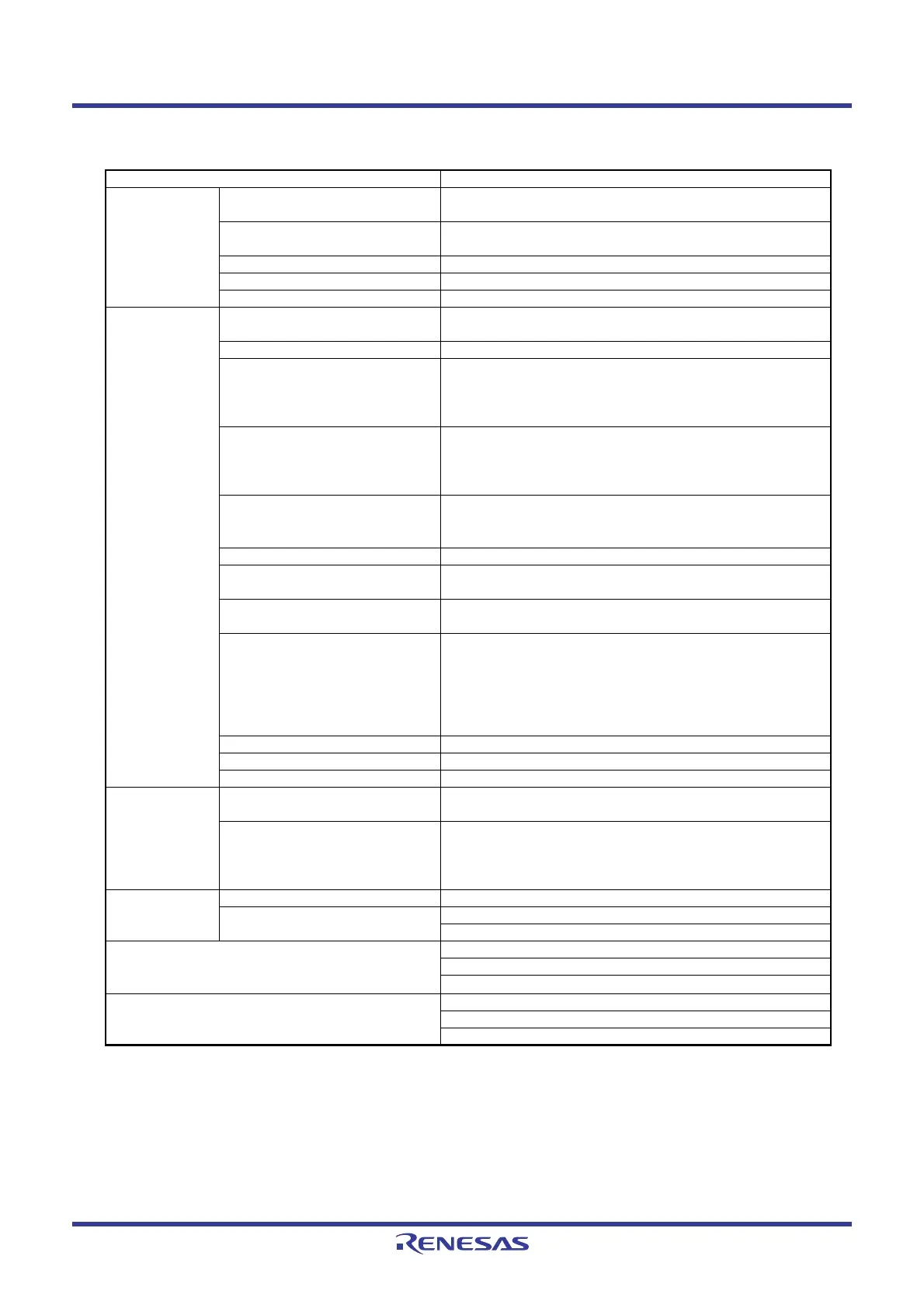
Table 1.2 Functions and Specifications for R8C/1B Group
Item Specification
CPU Number of fundamental
instructions
89 instructions
Minimum instruction execution
time
50 ns (f(XIN) = 20 MHz, VCC = 3.0 to 5.5 V)
100 ns (f(XIN) = 10 MHz, VCC = 2.7 to 5.5 V)
Operating mode Single-chip
Address space 1 Mbyte
Memory capacity See Table 1.4 Product Information for R8C/1B Group
Peripheral
Functions
Ports I/O ports: 13 pins (including LED drive port)
Input port: 3 pins
LED drive ports I/O ports: 4 pins
Timers Timer X: 8 bits × 1 channel, timer Z: 8 bits × 1 channel
(Each timer equipped with 8-bit prescaler)
Timer C: 16 bits × 1 channel
(Input capture and output compare circuits)
Serial interfaces 1 channel
Clock synchronous serial I/O, UART
1 channel
UART
Clock synchronous serial interface 1 channel
I
2
C bus Interface
(1)
Clock synchronous serial I/O with chip select (SSU)
A/D converter 10-bit A/D converter: 1 circuit, 4 channels
Watchdog timer 15 bits × 1 channel (with prescaler)
Reset start selectable, count source protection mode
Interrupts
Internal: 11 sources, External: 4 sources, Software: 4 sources,
Priority levels: 7 levels
Clock generation circuits 2 circuits
• Main clock generation circuit (with on-chip feedback
resistor)
• On-chip oscillator (high speed, low speed)
High-speed on-chip oscillator has a frequency adjustment
function
Oscillation stop detection function Main clock oscillation stop detection function
Voltage detection circuit On-chip
Power on reset circuit On-chip
Electric
Characteristics
Supply voltage VCC = 3.0 to 5.5 V (f(XIN) = 20 MHz)
VCC = 2.7 to 5.5 V (f(XIN) = 10 MHz)
Current consumption Typ. 9 mA
(VCC = 5.0 V, f(XIN) = 20 MHz, A/D converter stopped)
Typ. 5 mA
(VCC = 3.0 V, f(XIN) = 10 MHz, A/D converter stopped)
Typ. 35 µA (VCC = 3.0 V, wait mode, peripheral clock off)
Typ. 0.7 µA (VCC = 3.0 V, stop mode)
Flash Memory Programming and erasure voltage VCC = 2.7 to 5.5 V
Programming and erasure
endurance
10,000 times (data flash)
1,000 times (program ROM)
Operating Ambient Temperature -20 to 85°C
-40 to 85°C (D version)
-20 to 105°C (Y version)
(2)
Package 20-pin molded-plastic LSSOP
20-pin molded-plastic SDIP
28-pin molded-plastic HWQFN
 Loading...


